

Introduction to Plasma Etching
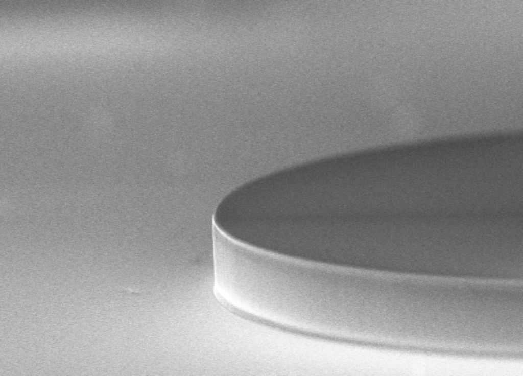
Plasma etching is a fundamental plasma technology used throughout modern semiconductor manufacturing and research in advanced microfabrication. As device dimensions continue to shrink into the micro- and nanometre range, plasma-based dry etching has become essential for achieving the precision, anisotropy, and material selectivity required for advanced microelectronics, nanotechnology, photonics, and optoelectronics.
Selecting the appropriate plasma etching technique depends on factors including feature size, aspect ratio, material system, surface quality, and production requirements. This article provides an overview of the principal plasma etching techniques. We will highlight operating principles, advantages, limitations, and typical applications for:
- Reactive Ion Etching (RIE),
- Inductively Coupled Plasma Reactive Ion Etching (ICP-RIE),
- Deep Reactive Ion Etching (DRIE), and
- Atomic Layer Etching (ALE),
Understanding Plasma Etching
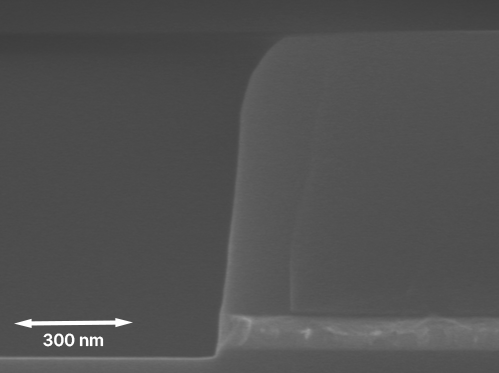
Plasma etching is a plasma-based process in which a low-pressure RF plasma is generated in a vacuum chamber to remove material from a substrate surface. The plasma contains reactive ions, radicals, electrons, neutral molecules, and ionised species. These are generated from gases such as fluorine- and chlorine-based chemistries. Material removal results from chemical reactions together with energetic ion bombardment, providing many of the benefits associated with ion beam processing while maintaining high throughput.
Compared with wet chemical etching, plasma etching provides superior pattern fidelity, excellent compatibility with photoresist and hard masks. It offers precise control when processing complex multilayer structures. By adjusting process parameters such as:
- Pressure
- RF power
- Gas composition
- Substrate bias
- Plasma density
Engineers can optimise etch rate, anisotropy, selectivity, and surface damage for specific applications.
Consequently, plasma etching is widely used in semiconductor devices, microelectromechanical systems (MEMS), photonics, quantum technologies, and advanced nanoelectronics.
How to Choose the Right Plasma Etching Technique
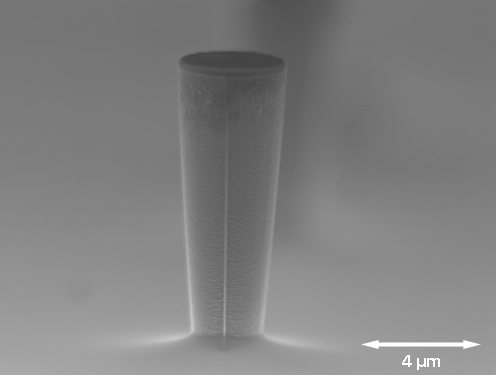
No single plasma etching technique is suitable for every application. The optimum process depends on the required
- Etch profile
- Material system
- Aspect ratio
- Surface quality
- Throughput
- Device architecture
Understanding the strengths and limitations of each technology enables the selection of the most appropriate process.
Comparing Reactive Ion Etching (RIE) and the ICP-RIE Process
How Does Reactive Ion Etching Work?
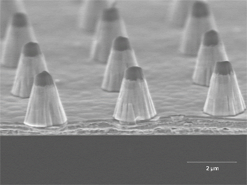
Reactive Ion Etching (RIE) is one of the most widely used plasma etching techniques in microfabrication. Conventional RIE systems employ a parallel-plate reactor in which RF power generates the plasma while simultaneously biasing the substrate. This accelerates ions towards the wafer surface, producing directional etching through a combination of chemical reactions and physical sputtering.
Why Choose RIE?
RIE provides a good balance between chemical selectivity and anisotropic etching while maintaining relatively simple hardware and straightforward process control. The technology is cost-effective and versatile, making it well suited to research laboratories and low-volume manufacturing.
Typical applications include the fabrication of electronic devices and integrated circuits based on silicon, silicon dioxide, silicon nitride, III–V semiconductors, and metals. In photonics, RIE is commonly used to fabricate waveguides, diffraction gratings, and photonic crystal structures. This is where moderate aspect ratios and accurate lateral dimensions are often required.
However, conventional RIE has several limitations. Plasma density is relatively low, restricting achievable etch rates and making the process less suitable for deep or high-aspect-ratio structures. Because plasma density and ion energy are directly coupled, increasing anisotropy often increases ion bombardment. This can reduce selectivity, erode masks, and introduce substrate damage. Process windows are also narrower for advanced nanoscale structures and heterogeneous material stacks, while microloading and wafer non-uniformity can become significant.
These limitations have driven the widespread adoption of high-density plasma technologies such as ICP-RIE.
What is ICP-RIE?
Inductively Coupled Plasma Reactive Ion Etching (ICP-RIE) is an advanced form of RIE that separates plasma generation from substrate bias. In systems such as the SENTECH SI 500, an inductively coupled RF source generates a high-density plasma, while an independent RF bias controls ion energy at the wafer surface.
What are the Advantages of ICP-RIE?
The independent control of plasma density and ion energy is the defining advantage of ICP-RIE. High plasma densities enable faster etch rates, while separate bias control allows excellent anisotropy, high selectivity, and reduced substrate damage. This combination makes ICP-RIE particularly suitable for advanced nanoscale fabrication.
ICP-RIE is widely used for semiconductor manufacturing, advanced plasma processing solutions, nanotechnology research, and compound semiconductor fabrication.
Typical applications include:
- High-aspect-ratio nanostructures
- GaN and SiC power devices
- LEDs
- Laser diodes
- Photonic devices,
- MEMS
- Quantum technologies
Research institutes also value ICP-RIE for its flexibility, reproducibility, and broad process capability.
The increased performance does come with greater system complexity and a wider process parameter space. Developing highly optimised processes therefore requires greater expertise than conventional RIE, although the resulting process performance is significantly improved.

What are the Key Features and Applications of DRIE and Cryogenic Etching?
When Should Deep Reactive Ion Etching (DRIE) Be Used?
Deep Reactive Ion Etching (DRIE) is a specialised plasma etching technique developed to produce extremely high-aspect-ratio structures, particularly in silicon. The most widely used implementation is the Bosch process, which alternates between etching and passivation cycles to produce near-vertical sidewalls.
DRIE enables etch depths of hundreds of micrometres while maintaining excellent profile control, making it indispensable for three-dimensional microfabrication. It also offers good wafer-scale uniformity and compatibility with standard lithographic masks.
The technology is widely used in MEMS fabrication for deep trenches, cavities, and through-silicon vias (TSVs). Typical applications include inertial and pressure sensors, RF MEMS, microfluidic devices, and advanced packaging. In photonics and micro-optics, DRIE is used to fabricate silicon structures for optical alignment, packaging, and integrated photonic devices.
Despite these advantages, Bosch DRIE has several limitations. It is primarily intended for silicon processing and produces characteristic sidewall scalloping caused by the alternating etch-passivation sequence.
Although acceptable for many MEMS applications, this roughness can increase optical scattering in photonic devices. DRIE can also exhibit aspect-ratio-dependent etching (ARDE), microloading, and pattern-density effects that reduce etch uniformity. Continuous high-density plasma processes have since been developed for additional materials, including SiC, quartz, technical glass, and compound semiconductors.
What are the Benefits of Cryogenic Plasma Etching?
Cryogenic plasma etching provides an alternative approach to producing highly anisotropic silicon structures with exceptionally smooth sidewalls. Instead of alternating etch and passivation cycles, the substrate is cooled to between approximately −80 °C and −140 °C, allowing a thin SiOxFy passivation layer to form naturally during the etch process.
This layer protects the sidewalls while ion bombardment continuously removes it from horizontal surfaces, enabling highly directional etching.
Silicon is typically etched using an SF₆/O₂ plasma while the wafer is cooled with liquid nitrogen. Unlike the Bosch process, cryogenic etching operates continuously without polymer deposition, eliminating scalloping and producing extremely smooth sidewalls.
This makes cryogenic etching particularly attractive for silicon photonics, optical waveguides, photonic crystal structures, high-Q resonators, MEMS, and emerging quantum devices, where surface roughness can significantly influence the performance of electronic and photonic devices.
However, cryogenic processing requires precise control of wafer temperature, helium backside cooling, and specialised chuck designs. It can also be more sensitive to wafer loading and pattern-density effects than Bosch DRIE. Since mask selectivity is generally lower, hard masks such as SiO₂ or Si₃N₄ are often preferred for deep or high-aspect-ratio structures.
What is Atomic Layer Etching (ALE)?
Atomic Layer Etching (ALE) represents the highest level of precision available in plasma etching. Rather than continuously removing material, ALE uses sequential self-limiting surface reactions to remove material one atomic layer at a time.
The primary advantage of ALE is exceptional control over etch depth, uniformity, and substrate damage. Because each reaction cycle removes only a controlled amount of material, ALE enables angstrom-level precision with excellent repeatability. This is particularly important for advanced semiconductor devices where even atomic-scale variations can influence electrical or optical performance.
When is ALE the Right Choice?
ALE is ideally suited to leading-edge semiconductor research, including advanced logic and memory devices, quantum technologies, heterogeneous integration, and next-generation optoelectronics. It is also attracting increasing interest for surface activation, photonics, nano-optics, and heterogeneous material integration, where its surface-smoothing capability can improve optical performance.
The principal limitation of ALE remains throughput. Since only one atomic layer is removed during each cycle, the process is inherently slower than conventional plasma etching and is therefore primarily used for research, process development, and selected high-value manufacturing applications.
Plasma Etching Tools from SENTECH
How Do SENTECH Plasma Etching Systems and Software Support Advanced Research and Manufacturing?
SENTECH offers a comprehensive portfolio of plasma etching systems for semiconductor research, micro- and nanofabrication, photonics, and optoelectronics. Platforms such as the SI 500 provide advanced plasma processing solutions supporting RIE, ICP-RIE, DRIE, and ALE in flexible standalone or cluster configurations.
Precise control of plasma density, ion energy, gas chemistry, pressure, and substrate temperature enables highly reproducible processes for advanced materials research and nanoscale device fabrication. The modular architecture allows systems to be configured for applications ranging from compound semiconductors and MEMS, metal surfaces, to quantum technologies and integrated photonics.
Modern plasma etching depends as much on advanced process software as it does on hardware. Sophisticated software enables precise control of process parameters, recipe management, automation, real-time monitoring, and comprehensive data logging, ensuring reproducible and efficient plasma processing. The SENTECH Intelligent Application (SIA) software platform combines these capabilities in an intuitive interface, helping researchers and manufacturers develop, optimise, and transfer plasma etching processes with confidence while maintaining consistent process quality.
With a strong focus on research and small- to medium-scale production, SENTECH supports customers from initial process development through to scalable manufacturing.
Our plasma processing and thin-film metrology application laboratories in Berlin provide expert support for process optimisation, sample evaluation, and application development, helping researchers accelerate the transition from laboratory innovation to industrial production.
Conclusion
Plasma etching remains one of the enabling technologies of modern semiconductor manufacturing. Whether the application requires the versatility of RIE, the high performance of ICP-RIE, the deep silicon structures produced by DRIE, or the atomic-scale precision of ALE, selecting the appropriate process is essential for achieving the required device performance.
By combining advanced plasma processing technologies with expert application support, SENTECH provides researchers and manufacturers with the tools needed to develop the next generation of semiconductor, photonic, MEMS, and quantum devices.