

MEMS Applications
Micro-electromechanical systems or MEMS is the umbrella term for many microfabricated devices that enable highly scalable, cost-efficient, mass-produced sensors, actuators, and optics. MEMS have many applications and are often found in for example pressure sensors, acceleration sensors, and microphones due to their extremely high sensitivity, small size, and very low power consumption and their suitability for integration with microelectronic systems.
Industries:
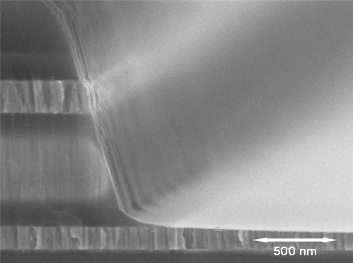
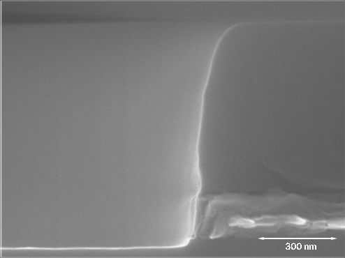
Conventional plasma etching processes are designed for etch depths of only a few microns and lack etch rate and mask selectivity. Deep reactive ion etching (DRIE) of silicon to create high aspect ratio microstructures is a key process in the advanced MEMS field. Two approaches are commonly known: the gas chopping process, the “Bosch process” and the cryogenic (cryo) etching. These processes are capable of producing deep features with exceptional anisotropy, etch rate, and etch mask selectivity. The Bosch process excels in etch rate and aspect ratio and is hence recognised as the main production technology. The cryo process overcomes the drawback of scalloping with the Bosch process and allows for smooth sidewalls.
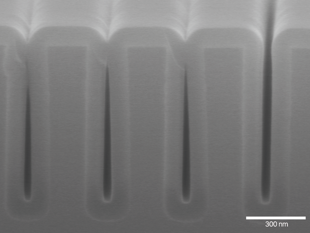
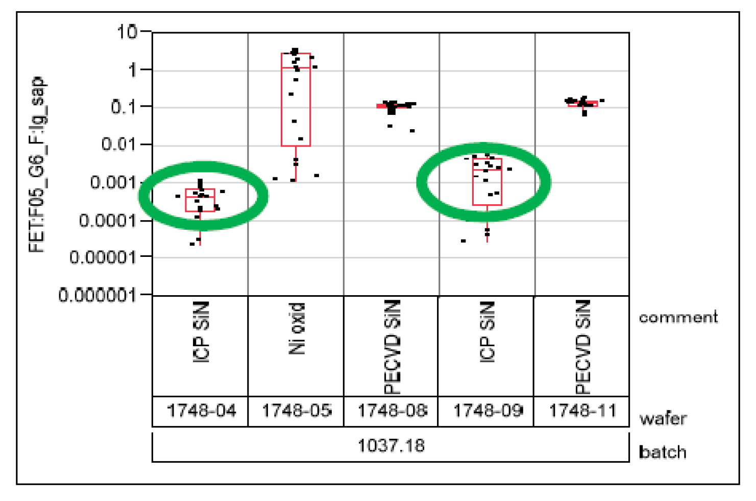
SENTECH ICP-RIE systems can be configured for DRIE using Bosch, cryo, or both processes. Additionally, the SENTECH SI 500 enables a new level of MEMS functionality, for leading-edge applications including AlN and AlScN piezo MEMS etching, and the SENTECH SI 500 D for the high-quality, precise stress-controlled ICPECVD of Si3N4 and SiO2 deposition.
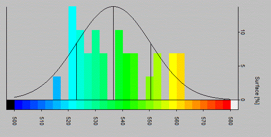
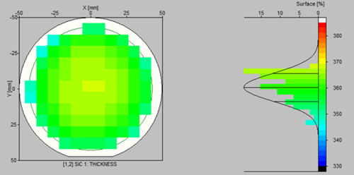
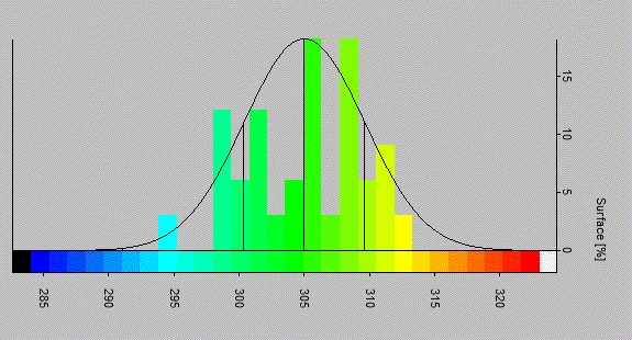
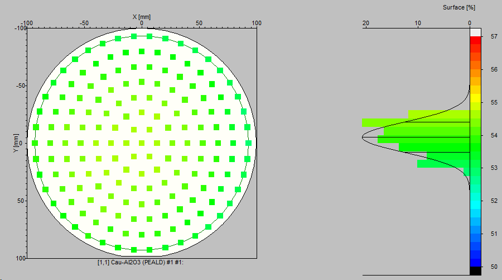
The SENTECH spectroscopic ellipsometry and reflectometry systems are ideally suited to characterise the quality of process steps on R&D and fully automated production level. Applying pattern recognition, they enable automated measurements of film thickness, optical constants, and the uniformity also of patterned wafers to gain insight into the development and stage of any MEMS devices.
Learn more about SENTECH plasma process technology, process monitoring, endpoint detection, and thin-film characterisation solutions by requesting the full application note.