


Quality Control

Optimise your etch and deposition processes for performance, reliability, and yield with precision thin film metrology tools for quality control.

SENTECH Instruments generic blue divider

Quality control

Quality control plays a crucial role in ensuring the reliability, performance, consistency of semiconductor etch and deposition processes. Using precision metrology tools ensures process optimisation. The SENTECH thin film metrology range of ellipsometers and reflectometers, in-situ, table top and fully automated tools for use in research and production can be used as part of your etch processes to  achieve low non-uniformity, selectivity, etch rate control and monitoring, endpoint detection and chamber contamination control and film thickness control, low non-uniformity, adhesion, conformity, chemical composition and stress control in your deposition processes.

Industries:
Electronics
Optics
Coatings
Sensors
MEMS and rf/power devices
Production

The SENTECH range of thin film metrology quality control tools offer precise measurements of refractive index and film thickness which is vital to the performance, reliability, and functionality of optical and electrical device properties such as lenses and filters. Our tools help to identify and correct any issues related to uneven deposition and process defects helping to minimise material waste and optimise cost efficiency.

Using the SENTECH tools for quality control in thin film metrology ensures consistent and reliable performance of thin film-based products across applications such as sensors, MEMS, and rf/power devices and maintains uniformity and durability during production.
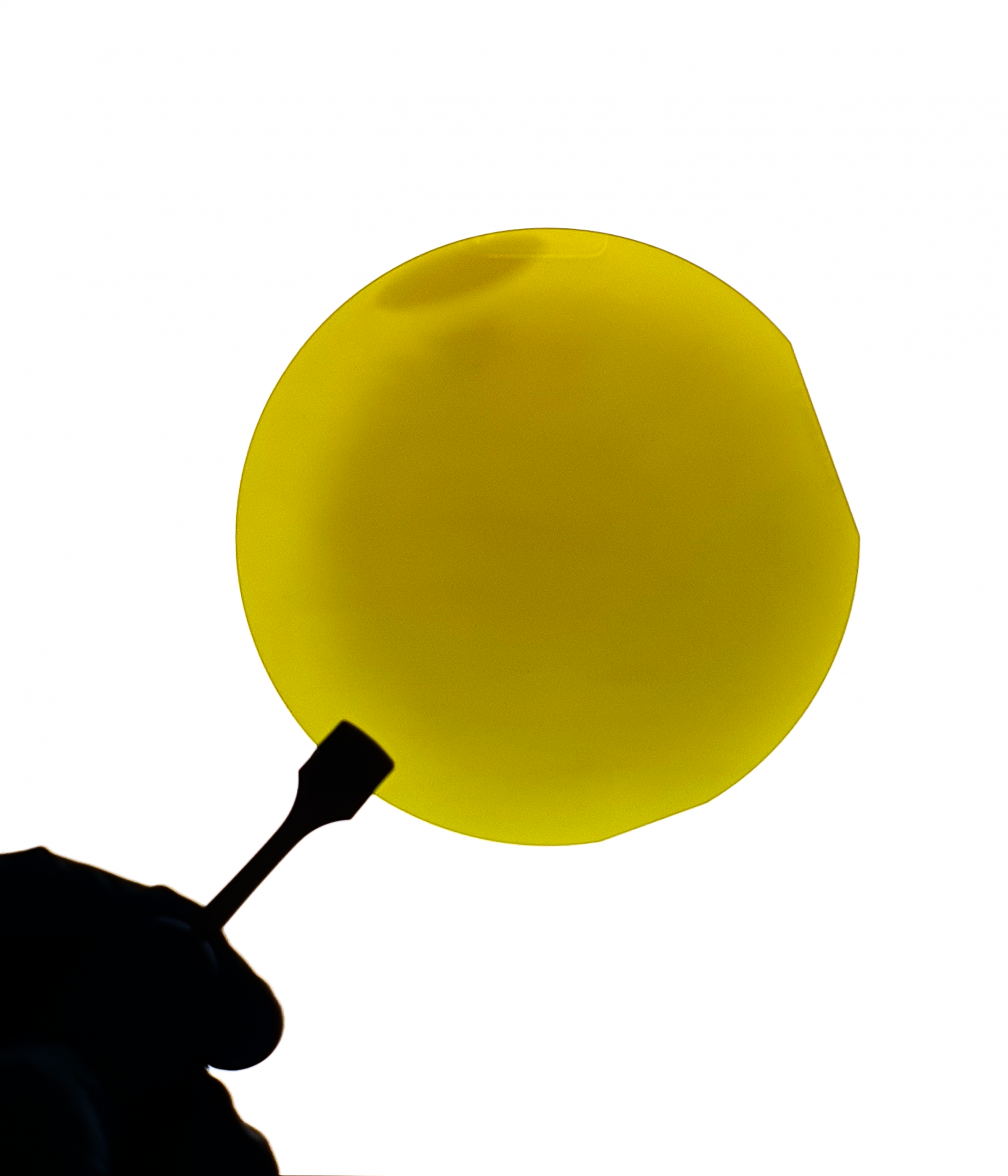
 

Quality Control of functional dielectric layers on SiC using the SENTECH SENDURO accuva10

SiC Wafer with no BSR
Quality Control of functional dielectric layers on SiC using the SENTECH SENDURO accuva10
Company name
Full name
Email address (business)
Phone number (optional)
Privacy policy
Position: 0
Slide to 5 to confirm you’re human.

Silicon carbide (SiC) possesses unique material properties such as high thermal conductivity, high breakdown voltage, and wide bandgap, making these substrates extremely suitable for applications in harsh environments where traditional silicon devices may not perform reliably. However, using SiC wafers presents process and application challenges. When used in conjunction with functional dielectric layers, e.g. silicon nitride (SiNₓ) and silicon dioxide (SiO₂) layers, SiC is ideal for high-power, high-frequency, and high-temperature applications in semiconductor devices used in power electronics, telecommunications, automotive electronics, and many other developing fields.
Precision characterisation of material defects, impurities, and interface properties helps to assess the reliability and yield of SiC-based semiconductor devices. Wafer thickness, however, can lead to some process challenges, which require precise process quality control and optimisation. Learn how using ellipsometric characterisation with the SENDURO accuva10 serves as a highly efficient quality control and process optimisation measure during the fabrication of dielectric layers and stacks in SiC-based devices.

Would you like more information?

Company name
Full name
Email address (business)
Location
Location of company
Privacy policy
Position: 0
Slide to 5 to confirm you’re human.