

SENTECH at NAPEX Virtual Symposium: Frontiers in Nanoscale Plasma Etching
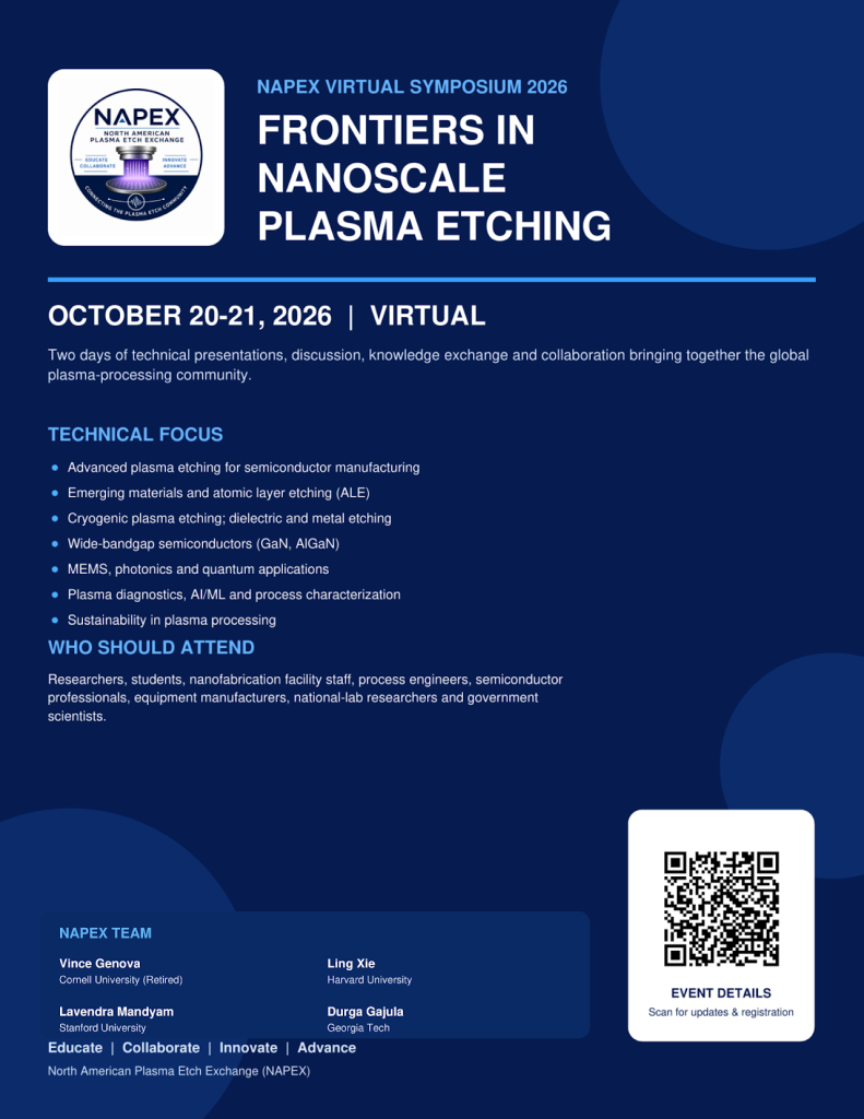
SENTECH is pleased to participate in the upcoming North American Plasma Etch Exchange (NAPEX) virtual symposium, “Frontiers in Nanoscale Plasma Etching”
20 – 21 October, 2026.
The two-day virtual symposium will bring together researchers and professionals from academia, industry, nanofabrication facilities, and the semiconductor community to exchange knowledge and discuss recent developments and emerging challenges in plasma etching and atomic layer processing.
Bringing together experts in plasma processing
The NAPEX symposium features invited speakers representing a broad range of leading companies, universities and research organisations, including Applied Materials, Silicon Austria Labs, Oxford Instruments, University of Nevada Reno, UC Berkeley, SENTECH, AlixLabs, Caltech, IonQ, Engenius Micro, Georgia Tech, and UCSB.
Across the two-day programme, presentations and discussions will address some of the most important developments in nanoscale plasma processing and semiconductor manufacturing.
Technical topics include:
- Atomic layer etching (ALE)
- Plasma-enhanced atomic layer processes
- Advanced semiconductor manufacturing
- Ferroelectric materials
- Wide-bandgap materials
- SiC processing
- Lithium niobate etching
- Diamond etching
- Advanced logic and memory technologies
- Emerging plasma-processing applications
SENTECH expertise in advanced plasma processing
As a manufacturer of advanced plasma process technology, SENTECH develops solutions for demanding research, development and semiconductor processing applications where precise control of material removal and surface properties is essential.
SENTECH plasma process systems support technologies including ICP-RIE, cryogenic ICP-RIE, atomic layer etching (ALE), ICP-PECVD and plasma-enhanced atomic layer deposition (PEALD).
These technologies address a wide range of emerging applications, from wide-bandgap semiconductor devices and advanced electronics to photonics, quantum technologies, MEMS and nanoscale device fabrication.
SENTECH’s participation in the NAPEX symposium provides an opportunity to exchange knowledge with the international plasma-processing community and contribute to discussions surrounding the next generation of nanoscale etching and atomic layer processing.
Who should attend?
NAPEX encourages participation from faculty, researchers, students, cleanroom and nanofabrication staff, process engineers, and semiconductor professionals. Participation in the virtual symposium is free of charge, making the event an excellent opportunity for the wider research and semiconductor communities to hear from experts working at the forefront of plasma etching and atomic layer processing. The organisers also encourage participants to share the event with colleagues, students, research groups and professional networks who may be interested in the programme.
Registration is free:
Register for the NAPEX Virtual Symposium
Full programme and event information:
Frontiers in Nanoscale Plasma Etching – Event Page
We look forward to joining the NAPEX community on October 20–21, 2026 and contributing to the exchange of ideas around the future of nanoscale plasma etching and advanced plasma processing.