Applications
Applications span an extensive range of film thicknesses, from ultra-thin 1 nm semiconductor and microelectronic layers such as SiO₂, Si₃N₄, graphene, and MoS₂, to photovoltaic materials including a-Si:H, perovskites, and TCOs. Spectroscopic ellipsometry can also characterise thicker films up to 15 μm, such as photoresist, nitride, and oxide layers (e.g., ZnO).
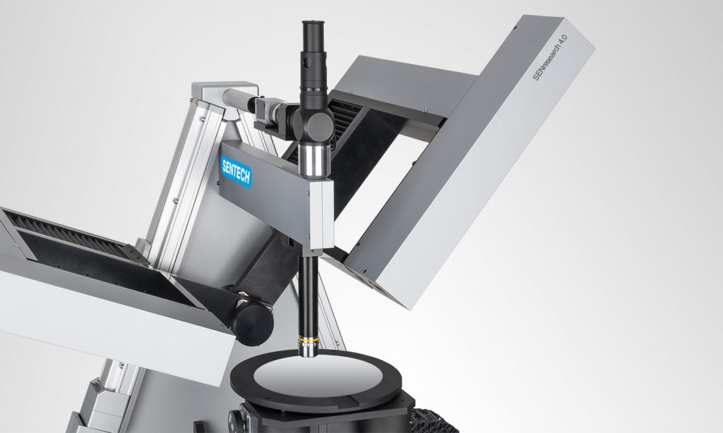
Discreet angle of incidence
The spectroscopic ellipsometer SENpro comprises a goniometer with discreet angles of incidence in 5°-steps (40° - 90°) to optimise the ellipsometric measurement.
Cost efficiency
The SENpro is a cost-effective spectroscopic ellipsometer without compromising advanced measurement performance.
Field upgradable accessories
Mapping Turntable for anisotropic samples 2C for full Mueller matrix measurement Video based auto-align Microspots Liquid cells Heating and cooling stage Transmission holder
Options
Manual goniometer Motorised Pyramid Goniometer In situ, in line, and desktop Reflectometer
Spectral ranges
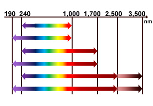
DUV – VIS 190 – 1,000 nm 240 – 1,000 nm NIR with Diode-Array 190 – 1,700 nm 240 – 1,700 nm NIR with FTIR 190 – 2,500 nm 190 – 3,500 nm 240 – 2,500 nm 240 – 3,500 nm
Spectral extension
A spectral extension of specular reflection into the NIR is available for the SENTECH SENsol.
Options
200 mm or 300 mm x-y mapping stage Extended spectral range to the NIR Reduced spot size optics, allows measurement inside squares less than 90 μm Option to measure wafer bow and stress Software interface to MES using SEC/GEM protocol
SI 591 reverse
RIE plasma etch with a small footprint Load lock for through-the-wall integration Halogen and fluorine chemistry For up to 200 mm wafers Diagnostic windows for laser interferometer and OES
Edge Grip
Minimum edge exclusion Flexibility for multiple wafer sizes with quick change