Sensors

Learn how SENTECH plasma systems and metrology tools are ideal for processing advanced sensor applications.

SENTECH Instruments generic blue divider

Sensor Applications

Sensor applications are used in devices that detect and measure physical properties or changes in the environment and convert them into electrical signals. These properties can include light, temperature, pressure, humidity, motion, and more. Detection speed, efficiency, and small size make these devices highly suitable for use in many leading-edge and growing industrial applications. SENTECH systems and tools are used in key types of sensing technology, including photodetectors, gas sensing and quantum sensing.

Industries:
Industrial electronics
Electronic communications
Medicine & healthcare
Analytical equipment
Automotive & transport
Healthcare

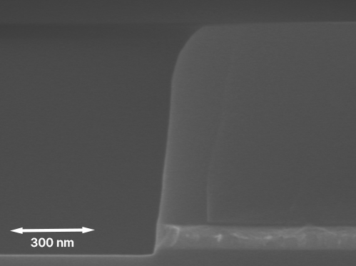
Photodetectors are devices designed to detect and measure light or photons. They convert incoming photons into electrical signals that can be processed and analysed.  Photodetectors serve as the light-sensitive component in optical sensors. When integrated into a sensor system, they enable the detection and measurement of light intensity, color, or the presence of specific wavelengths.

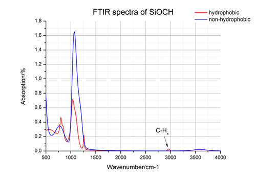
Gas sensing involves the detection and measurement of the presence and concentration of gases in the surrounding environment. This is crucial in various fields such as environmental monitoring, industrial safety, healthcare, and more. Sensors play a fundamental role in gas sensing by converting the physical or chemical changes associated with the presence of a specific gas into measurable signals.

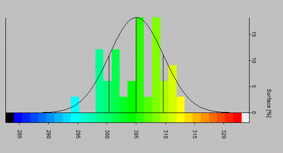
Quantum sensing leverages the principles of quantum mechanics to achieve highly sensitive measurements. In the context of sensors, quantum sensing refers to the use of quantum properties to enhance the precision and sensitivity of sensing devices.

Learn more about SENTECH plasma process technology, process monitoring, endpoint detection, and thin-film characterisation solutions by requesting the full application note.

Diamond Etching for Quantum Computing and Sensing using the SENTECH SI 500 ICP-RIE System

Isotropic etch of a free-standing diamond waveguide

Diamond Etching for Quantum Computing and Sensing using the SENTECH SI 500 ICP-RIE System

Company name
Full name
Email address (business)
Phone number (optional)
Privacy policy
Position: 0
Slide to 5 to confirm you’re human.

Low-damage plasma etching is crucial for the fabrication of diamond-based quantum technologies, such as quantum computing and quantum sensing. The unique properties of diamond, such as its long spin coherence time and its ability to host nitrogen-vacancy (NV) centres, make it an excellent candidate for use in quantum applications. The NV centres can be used as qubits in quantum computing and for sensing weak magnetic and electric fields. Isotropic and anisotropic plasma etching are necessary to produce tailored diamond structures for various applications. Inductively coupled plasma reactive ion etching (ICP-RIE) is a preferred method for diamond plasma etching due to its high selectivity, low non-uniformity, and low damage.

Low-Temperature ICPECVD of Si₃N₄ Films using the SENTECH SI 500 D System

Si3N4 thickness uniformity

Low-Temperature ICPECVD of Si₃N₄ Films using the SENTECH SI 500 D System

Company name
Full name
Email address (business)
Phone number (optional)
Privacy policy
Position: 0
Slide to 5 to confirm you’re human.

Silicon Nitride (Si₃N₄) layers are extensively used as passivation layers, etching masks, membranes, electrically isolating layers, and dielectrics for leading-edge applications, including microelectronic devices, sensors, and OLEDs. This application note demonstrates the successful inductively coupled plasma-enhanced chemical vapour deposition (ICPECVD) process results inSi₃N₄ films with excellent uniformity, high growth rate, and adjustable low film stress using the SENTECH SI 500 D ICPECVD System.

Low-Damage Etching of AlGaN Open Gate Layer in AlGaN/GaN Sensor for Detecting NO₂ using the SENTECH SI 500 ICP-RIE System

The PTSA ICP source provides stable processing conditions

Low-Damage Etching of AlGaN Open Gate Layer in AlGaN/GaN Sensor for Detecting NO₂ using the SENTECH SI 500 ICP-RIE System

Company name
Full name
Email address (business)
Phone number (optional)
Privacy policy
Position: 0
Slide to 5 to confirm you’re human.

This application note will demonstrate how a process was developed and carried out using the SENTECH SI 500 ICP-RIE Etch System configured with the Planar Triple Spital Antenna (PTSA) inductively coupled plasma (ICP) source for low-damage etching of sensitive AlGaN/GaN Heterostructure for Nitrogen dioxide (NO₂) gas sensing. NO2 continues to be a significant environmental pollutant. The demand for selective, continuous, parts-per-billion (ppb)-level monitoring of NO₂ using low-power sensors suitable for integration into smart sensor networks remains high.

Traditional devices, such as those based on In₂O₃, SnO₂, ZnO, InAs, InP, WO₃, and acoustic wave sensors, have faced challenges including reproducibility, high power consumption,
and limited lifespans. Despite recent advancements in developing high-performance NO₂ sensors, many devices are still not mature enough for widespread deployment. However, Heterostructures based on AlGaN/GaN continue to show great promise as a generic platform for developing high-performance sensing devices that offer direct electrical readout. These devices utilise the sensitivity of the highly mobile two-dimensional electron gas (2DEG) formed at the AlGaN/GaN heterostructure interface to changes in polarisation or surface charge.

Low-Damage Etching of Al Layers on Si for Advanced MEMS Sensors and Quantum Device Fabrication using the SENTECH SI 500 ICP-RIE System

Al layers on Si vertical sidewalls

Low-Damage Etching of Al Layers on Si for Advanced MEMS Sensors and Quantum Device Fabrication using the SENTECH SI 500 ICP-RIE System

Company name
Full name
Email address (business)
Phone number (optional)
Privacy policy
Position: 0
Slide to 5 to confirm you’re human.

Aluminium (Al) is a key material in advanced semiconductor, MEMS sensors, and quantum device fabrication, where low interface roughness, vertical sidewall profiles, and stringent etch uniformity are critical for device performance and yield. In particular, Al-on-Silicon (Si) processes used in superconducting quantum circuits, high-frequency devices, and precision sensors place stringent demands on plasma etching to minimise substrate damage and maintain reproducible feature geometry. This application note demonstrates a robust, low-damage, inductively coupled plasma  reactive ion etching (ICP-RIE) process for Al layers on a 100 mm Si wafer using the SENTECH SI 500 ICP-RIE system. The process achieves smooth underlying Si surfaces after Al removal, vertical sidewalls, and an Al etch depth non-uniformity of ±2% across the wafer, including over-etch, highlighting the capability of the SI 500 for demanding Al etch applications.

Low-Temperature ICPECVD of SiO₂ Films using the SENTECH SI 500 D System

Deposition on SiO2 thickness mapping

Low-Temperature ICPECVD of SiO₂ Films using the SENTECH SI 500 D System

Company name
Full name
Email address (business)
Phone number (optional)
Privacy policy
Position: 0
Slide to 5 to confirm you’re human.

Silicon Oxide (SiO₂) layers are extensively used as passivation layers, etching masks, membranes, electrically isolating layers, and dielectrics for leading-edge applications, including microelectronic devices, sensors, OLEDs. This application note demonstrates the successful inductively coupled plasma-enhanced chemical vapour deposition (ICPECVD) process results in SiO₂ films with excellent uniformity, high growth rate, and adjustable low film stress using the SENTECH SI 500 D ICPECVD System.

Low-Damage Etching of Nb for Superconducting Quantum Devices using the SENTECH SI 500 ICP-RIE System

Etched Nb layers on Si with vertical sidewall

Low-Damage Etching of Nb for Superconducting Quantum Devices using the SENTECH SI 500 ICP-RIE System

Company name
Full name
Email address (business)
Phone number (optional)
Privacy policy
Position: 0
Slide to 5 to confirm you’re human.

Niobium (Nb) is a critical material for superconducting quantum circuits and devices, where low microwave loss, smooth interfaces, and well-controlled feature geometry are essential for achieving long coherence times and high device yield. Nb-on-silicon (Si) fabrication places stringent demands on plasma etching, requiring low substrate damage, vertical sidewalls, and excellent etch uniformity across the wafer.
This application note is a comparative study on chlorine (Cl) and fluorine (F) etch chemistries for low-damage ICP-RIE processes for Nb films on 100 mm Si wafers developed on the SENTECH SI 500 ICP-RIE system. We will demonstrate successful etching processes for smooth underlying Si surfaces after Nb removal with vertical sidewall profiles, and low etch depth non-uniformity across the wafer, including over-etch with both chemistries. Based on our results, we will illustrate the suitability of the SI 500 for quantum device fabrication.

HMDSO-Based ICPECVD of Hydrophobic Films using the SENTECH SI 500 D System

FTIR spectra of SiOₓCHy using SENTECH SENDIRA

HMDSO-Based ICPECVD of Hydrophobic Films using the SENTECH SI 500 D System

Company name
Full name
Email address (business)
Phone number (optional)
Privacy policy
Position: 0
Slide to 5 to confirm you’re human.

In this application note, we demonstrate the successful low-temperature Hexamethyldisiloxane (HMDSO)-based ICPECVD processes for hydrophobic SiOₓCHy films on Titanium Nitride (TiN)/Glass and TiN/Chromium Oxynitride (CrON)/Glass substrates using the SENTECH SI 500 D ICPECVD Plasma System. Furthermore, we evaluate the influence of plasma pre-treatment and RF substrate bias on adhesion and film performance. Organosilicon SiOₓCHy films are widely used as hydrophobic and protective coatings in microelectronic, optical and sensor applications. In many of these applications, coatings must be deposited on heterogeneous substrate stacks combining conductive metal layers with insulating glass. Such configurations place high demands on film uniformity, adhesion and mechanical stability. In particular, coatings on TiN/glass substrates require excellent interfacial bonding to the metal while maintaining homogeneous film properties across both conductive and insulating regions. HMDSO is a well-established precursor for the deposition of hybrid SiOₓCHy films by ICPECVD. Due to its organosilicon structure, HMDSO enables the formation of carbon-containing silicon oxide networks whose composition and surface properties can be adjusted by using specific plasma parameters.

ICPECVD of Silicon Nitride Films with Low-Hydrogen using the SENTECH SI 500 D System

Drain leakage current of the GaN HEMT with ICPECVD

ICPECVD of Silicon Nitride Films with Low-Hydrogen using the SENTECH SI 500 D System

Company name
Full name
Email address (business)
Phone number (optional)
Privacy policy
Position: 0
Slide to 5 to confirm you’re human.

Silicon Nitride (SiₓNy) layers are extensively used as passivation layers, etching masks, membranes, electrically isolating layers, and dielectrics for microelectronic devices, sensors, OLEDs, and much more. The hydrogen incorporation in SiₓNy films plays a very important role in the mechanical, chemical, and electrical properties and their long-term stability. Therefore, the performance of the devices using SiₓNᵧ films is very much influenced by this hydrogen incorporation. The proprietary plasma source PTSA 200 and the separation of gas inlets of SENTECH ICPECVD allow the deposition of SiₓNy films with low hydrogen concentration. SiₓNy deposited at low temperature in the SENTECH SI 500 D ICPECVD tool with low hydrogen content have been successfully demonstrated using SiH₄/NH₃ chemistry. Impressive applications of such ICPECVD films with low hydrogen content have been demonstrated by Fraunhofer IAF Freiburg (Germany) for gate passivation of GaN HEMTs and the use as dielectric of MIM capacitors.

Would you like more information?

Company name
Full name
Email address (business)
Location
Location of company
Privacy policy
Position: 0
Slide to 5 to confirm you’re human.