Power Devices

Learn more about GaN and SiC, the materials supporting this emerging technology in the semiconductor industry.

SENTECH Instruments generic blue divider

Power Device Applications

Power device applications and RF device technology are emerging as the future of power converters and systems industries, integrated devices, and 5G implementation. These devices have the advantage of being able to precisely control electrical energy from the source to the load according to the load demand, at high efficiency, and with outstanding reliability. Demand is growing due to their suitability to business areas including energy storage, power supplies, renewable energies, automotive and e-mobility, and mobile technologies.

Industries:
Energy storage
Power supplies
Renewable energies
Automotive and e-mobility
Mobile technologies

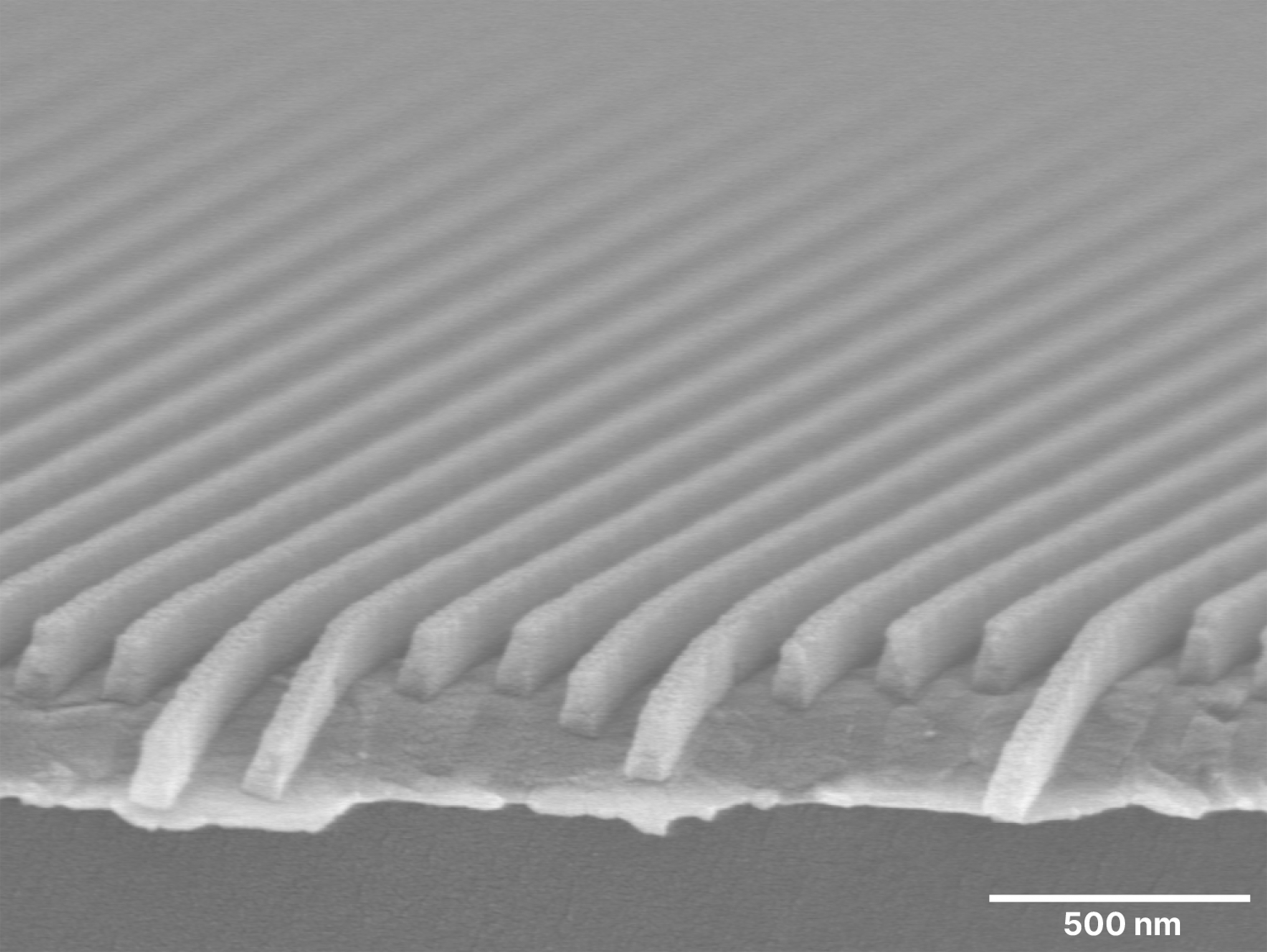
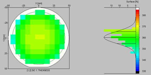
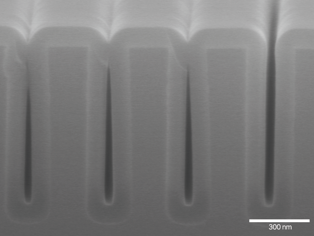
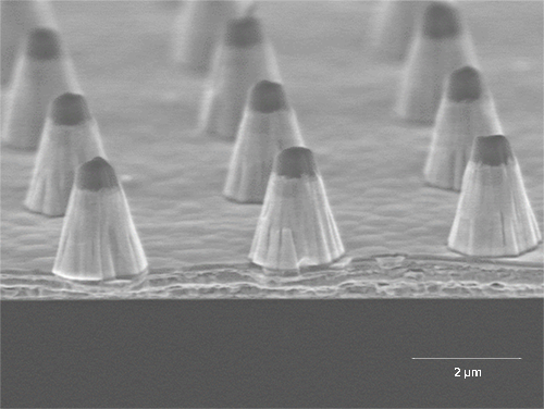
The SENTECH low-damage plasma processing capabilities provide leading-edge solutions for challenging SiC-based devices, AlGaN/GaN for HEMT devices, and High-K dielectrics as gate materials, as well as many applications in power electronics and high-frequency RF devices.

Our plasma process systems support high etch selectivity, low volatility of etch by-products on the substrate surface and sidewalls, and unwanted micro-masking.

Scroll down to read our literature and request copies of the full application notes or a brochure.

Please read our full article “Processing Silicon Carbide (SiC), Understanding the Challenges and Finding Pathways to Precision” to learn how SENTECH plasma process and thin-film metrology systems are meeting the process and characterisation challenges for modern power devices.

SENTECH Solutions SiC Brochure

Request a copy of our brochure, which looks at how SENTECH offers a holistic approach to the reliable processing and accurate characterisation of SiC. Your request will be sent directly to our marketing team, who will deal with your brochure request. 

Etching of Aluminium (Al) Nanostructures using the SENTECH SI 500 ICP-RIE System

SiO2 etched at a rate of 60 nm/min and a selectivity of 1.4:1 to photoresist
Etching of Aluminium (Al) Nanostructures using the SENTECH SI 500 ICP-RIE System
Company name
Full name
Email address (business)
Phone number (optional)
Privacy policy
Position: 0
Slide to 5 to confirm you’re human.

This application note will demonstrate how a process was developed and carried out using the SENTECH SI 500 ICP-RIE System for the successful etching of Aluminium (Al) nanostructures. This process is essential in the semiconductor landscape for driving advancements in modern device performance, reliability, and miniaturisation. Al nanostructures possess exceptional electrical and thermal conductivity, making them ideal for a variety of applications, from enhancing barrier layers in multi-layer structures to improving low-resistance pathways in high-speed devices. Key roles in metal oxide semiconductor field effect transistors (MOSFETs), thin-film transistors (TFTs) for LCDs and OLEDs, and capacitors showcase the versatility of Al in modern electronics. Al nanostructures are set to shape the future of integrated circuits and power electronics, solidifying their position as a cornerstone of cutting-edge semiconductor technology. In this application note, we will demonstrate how the SENTECH SI 500 ICP-RIE Plasma Etch System successfully etched Al layers with a good profile, excellent selectivity to mask, and a good etch stop on the Al layer.

ICPECVD of Silicon Carbide Films using the SENTECH SI 500 D System

ICPECVD of SiC mapping
ICPECVD of Silicon Carbide Films using the SENTECH SI 500 D System
Company name
Full name
Email address (business)
Phone number (optional)
Privacy policy
Position: 0
Slide to 5 to confirm you’re human.

Amorphous Silicon Carbide (a-SiC:H) films are extensively used in solar cells and as passivation layers in sensors for high-temperature applications. In addition, thanks to its good mechanical properties and chemical resistance silicon carbide (SiC) is widely used as a protection layer against abrasion and chemical corrosion such as in MEMS applications. This application note will demonstrate the successful deposition of a-SiC:H layers using the SENTECH SI 500 D ICPECVD System. The procedure comprises the deposition of a-SiC:H layers by ICPECVD on a silicon wafer with a thickness in the range of ca. 200-600 nm with different process conditions. Characterisation was done by determining the optical layer properties using ellipsometry and measurement of the layer stress. The results demonstrate the excellent deposition properties of an SI 500 D system with a SiH₄/CH₄-based deposition process for a-SiC:H films.

PEALD of SiO₂ for Highly Conformal Trench Filling at Low Temperatures Using the SENTECH SI PEALD System

PEALD of SiO2 conformal trench fill
PEALD of SiO₂ for Highly Conformal Trench Filling at Low Temperatures Using the SENTECH SI PEALD System
Company name
Full name
Email address (business)
Phone number (optional)
Privacy policy
Position: 0
Slide to 5 to confirm you’re human.

This application note highlights the successful utilisation of the SENTECH SI PEALD system to perform a low-damage, low-temperature, and highly conformal trench-fill deposition process for silicon oxide (SiO₂) layers. Plasma-enhanced atomic layer deposition (PEALD) of SiO₂ is a state-of-the-art technique that achieves highly conformal and uniform film deposition, even within complex geometries like trenches, where precise control over thickness and coverage is essential.

Trenches and gratings are a cornerstone of modern semiconductor fabrication, enabling advancements in device scaling, performance, and reliability. The ability to perform conformal trench filling using PEALD of SiO₂ is critical for addressing challenges in creating smaller, faster, and more efficient semiconductor devices. The SENTECH SI PEALD system excels in delivering the precision and uniformity required for such processes, ensuring optimal film quality at low deposition temperatures.

This approach is particularly beneficial in advanced microfabrication and high-performance semiconductor devices across foundational and emerging industries. Applications include Quantum Devices, where precise interfaces are vital, Microelectromechanical Systems (MEMS), requiring robust dielectric layers, Photonic Integrated Circuits (PICs), which demand low-loss optical claddings, and Power Electronics, where high-quality dielectric isolation enhances device reliability.

Etching of GaN Structures with an SiO₂ Hard Mask using the SI 500 ICP-RIE System

SEM cross-section images of the etched GaN structures with SiO₂ and the remaining PR mask, with a profile angle of 74° to 75°
Etching of GaN Structures with an SiO2 Hard Mask using the SI 500 ICP-RIE System
Company name
Full name
Email address (business)
Phone number (optional)
Privacy policy
Position: 0
Slide to 5 to confirm you’re human.

In this application note, we will demonstrate that using the SENTECH SI 500 ICP-RIE System, we successfully developed a plasma etching process for GaN conical structures using a SiO₂ hard mask. The goal of the process development was to achieve GaN cone structures with a sidewall angle close to 75° while maintaining selectivity to mask and uniformity. Gallium nitride (GaN) is a key material for lasers, LEDs, optoelectronic and power electronic devices due to its wide bandgap, high breakdown field, thermal stability and efficient light emission. Fabrication of advanced GaN-based devices often requires highly controlled plasma etching processes capable of producing well-defined structures with steep sidewall angles and high mask selectivity. Inductively coupled plasma reactive ion etching (ICP-RIE) using chlorine(CI)-based chemistries is widely used for GaN pattern transfer due to its capability for high etch rates and anisotropic profiles.

Would you like more information?

Company name
Full name
Email address (business)
Location
Location of company
Privacy policy
Position: 0
Slide to 5 to confirm you’re human.