Options
Mapping (up to 200 x 200 mm2) Second objective lens SprectraRay/4 software PC
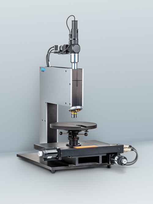
FTPadv EXPERT
Material database including: Dielectrics on semiconductors, Epitaxial films on semiconductors Metallic films on semiconductors Films on metallic substrates Films on transparent substrates
RM 2000
Spectral range: 200 nm - 1000 nm Film thickness range: 2 nm – 50 µm Spot size: 100 µm
RM 1000
Spectral range: 410 nm - 1000 nm Film thickness range: 20 nm – 100 µm Spot size: 80 µm
SE 401adv
In-situ laser ellipsometer with a time resolution of 40 ms. HeNe-laser for high stability and reproducibility Kit for easily mounting the sender and receiver modules to the flanges of a process chamber
SE 400adv
Table top equipment HeNe-laser for high stability and reproducibility Highly precise sample alignment Manual goniometer with superior performance and angle accuracy
Options
Mapping up to 200 mm, Liquid cells for in situ measurement, Video camera, Autofocus, Motorised goniometer, SpectraRay 4.0 simulation software, Certified standard wafer
Measurement parameters
Sample information Angle of incidence: multiple or single angle measurement Wavelength range Measurement mode: (ψ,Δ), (S1, S2), T, Rp, Rs Mapping options
Dispersion models
Brendel oscillator Cauchy Cody-Lorentz Drude-Lorentz oscillator Effective medium and index gradient Extended Drude Formula Forouhi-Bloomer Hamberg Harmonic oscillator Sellmeier Sernelius Spectrum combination Tanguy Tauc-Lorentz Uniaxial & biaxial anisotropic and others
Simulation parameters
Ellipsometric parameter ψ, Δ, tan (ψ), cos (Δ) Fourier coefficients Reflectance R, Rp, Rs Transmittance T Optical properties n, k, ne, no, ke, ko Material properties ε1, ε2 MSE value Colour values