Optoelectronics

Learn how SENTECH plasma systems and metrology tools are ideal for processing advanced optoelectronics applications.

SENTECH Instruments generic blue divider

Optoelectronic Applications

Optoelectronic applications combine electronic and photonic technologies to generate, manipulate, and detect light. Applications such as VCSELs, micro-LEDs, waveguides, and microlenses are becoming increasingly important in advanced sensing, communication, display, and imaging systems.  Optoelectronic applications are driven by growing demand from the aerospace, automotive, consumer electronics, information technology, telecommunications, and healthcare sectors. Optoelectronic applications continue to be one of the fastest-growing fields within semiconductor and photonic device manufacturing.

Industries:
Aerospace
Space
Automotive
Consumer electronics
Information technology
Healthcare

The SENTECH plasma product family provides highly effective solutions for many leading-edge optoelectronic applications. The SENTECH SI 500 D ICPECVD system can be used for high-quality dielectric deposition and trench filling for Micro LED applications, supporting the fabrication of advanced flat-panel display technologies.

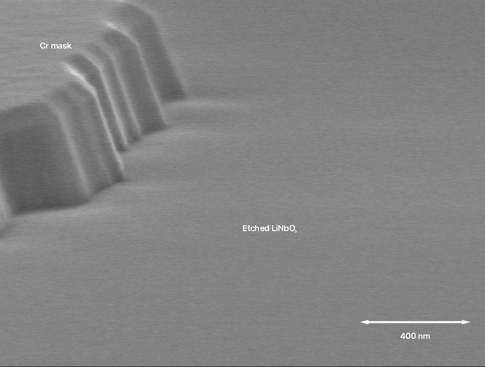
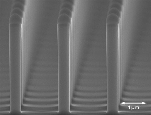
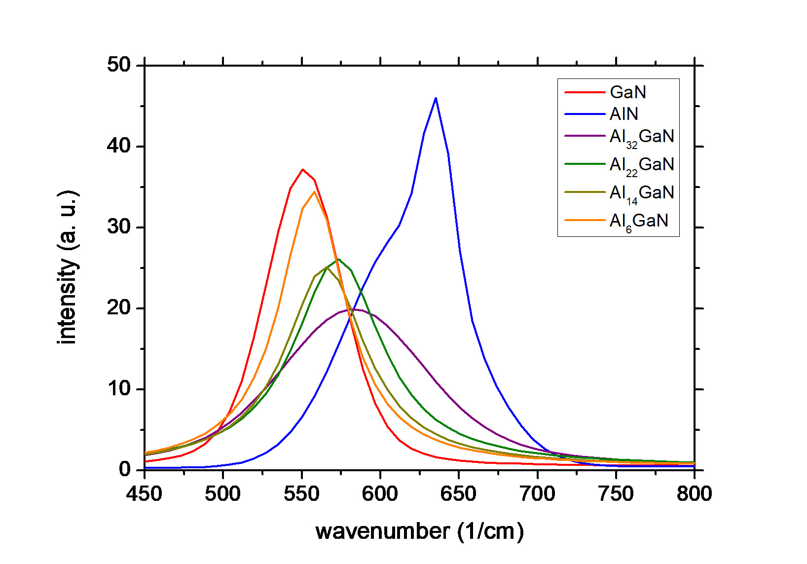
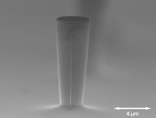
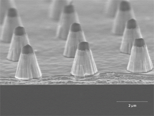
The SI 500 ICP-RIE plasma etch system with the PTSA source offers highly selective, low-damage etching with accurate endpoint detection for the fabrication of vertical and tapered GaAs-based VCSEL structures. The SENTECH SI 500 ICP-RIE system equipped with the Planar Triple Spiral Antenna (PTSA) 200 also enables low-damage etching of GaN- and InP-based devices for the fabrication of waveguides, photonic structures, and microlenses. Microlenses can significantly improve light extraction efficiency in LED devices or be used to focus and direct light in advanced photonic systems. Smooth, vertical, low-loss waveguides and facets for efficient optical coupling have also been demonstrated in materials such as SiN and SiO₂.

For advanced optoelectronic and photonic device fabrication, the SENTECH SI PEALD system enables the low-temperature deposition of high-quality thin films with atomic-scale thickness control. Plasma-Enhanced Atomic Layer Deposition (PEALD) is particularly well suited to the deposition of conformal dielectric, passivation, and functional layers on complex three-dimensional device structures. Typical applications include Micro LEDs, VCSELs, photonic integrated circuits (PICs), waveguides, optical coatings, and next-generation semiconductor devices, where precise film thickness, excellent uniformity, and superior interface quality are critical to device performance.

Learn more about SENTECH plasma process technology, process monitoring, endpoint detection, and thin-film characterisation solutions by requesting the full application note.

ICP Etching of Lithium Niobate (LiNbO₃) using the SENTECH SI 500 ICP-RIE System

Etching of LiNbO3

ICP Etching of Lithium Niobate (LiNbO₃) using the SENTECH SI 500 ICP-RIE System

Company name
Full name
Email address (business)
Phone number (optional)
Privacy policy
Position: 0
Slide to 5 to confirm you’re human.

Lithium Niobate (LiNbO₃, or LN) is a non-linear crystal material exhibiting properties such as large electro-optic coefficients, piezoelectric properties, large transparency range, and wide intrinsic bandwidth. Furthermore, LiNbO₃ on insulator (LNOI) will allow the fabrication of high-contrast optical waveguides, and high integration density photonics integrated circuits (PICs), and thus, finally open a new generation of miniature RF modulators.

The etching of smooth ridge waveguides is the most crucial step to fabricate PICs. As LiNbO₃ is a relatively hard crystal material, dry etching often results in high surface roughness and re-deposition on sidewalls, which leads to optical losses and poor device characteristics. Sulfur Hexafluoride (SF₆) gas or SF₆/Argon (Ar) mixing gas is widely used in plasma processes, and specifically SF₆/Ar gas mixture has been used to etch LiNbO₃.

Due to the low volatility of LiF and NbFₓ, a high bias power is necessary for physically-assisted desorption of such non-volatile fluorides to avoid surface roughening via micro-masking. This application note presents a successful etching of LiNbO₃ ridge waveguides with smooth sidewalls using a Chromium (Cr) mask due to its ability to withstand high bias power without compromising the profile and selectivity. An etch process based on a mixture of SF₆/Ar has delivered smooth ridge waveguide etching of LiNbO₃ without any re-deposition on sidewalls.

Etching of InP Pillars using the SENTECH SI 500 ICP-RIE System

Etching of InP pillars

Etching of InP Pillars using the SENTECH SI 500 ICP-RIE System

Company name
Full name
Email address (business)
Phone number (optional)
Privacy policy
Position: 0
Slide to 5 to confirm you’re human.

This application note will demonstrate the successful etching of Indium Phosphide (InP) pillars with near-vertical edge profile using the SENTECH SI 500 ICP-RIE system. Two-dimensional photonic crystals (PhCs) offer a huge potential in photonic integrated circuits. They can be used to miniaturise existing integrated optical devices, e.g., bends, microcavities, add-drop filters, and band edge lasers. The polarisation sensitivity of PhCs makes it possible to significantly reduce the footprint of polarisation filters. InP technology is the only platform to monolithically integrate active and passive devices for use in the telecom wavelength window (1530 nm to 1570 nm).

Aluminium Gallium Nitride Composition Analysis via PEALD on Sapphire using the SENTECH SI PEALD System

PEALD of AlGaN

AlxGa1-xN Composition Analysis via PEALD on Sapphire using the SENTECH SI PEALD System

Company name
Full name
Email address (business)
Phone number (optional)
Privacy policy
Position: 0
Slide to 5 to confirm you’re human.

This application note demonstrates the successful development of several reliable plasma-enhanced atomic layer deposition (PEALD) processes for aluminium gallium nitride (AlₓGa₁₋ₓN) thin films with different aluminium contents using the innovative SENTECH SI PEALD system with a PTSA ICP source, with a film thickness of below 20 nm. AlₓGa₁₋ₓN thin films require precise control over composition and uniformity to meet the performance demands of advanced optoelectronic and high-frequency electronic devices. In particular, the aluminium mole fraction (x) strongly influences the alloy’s optical bandgap and refractive index, making its accurate determination critical for process optimisation. This application note focuses on the deposition of AlₓGa₁₋ₓN on sapphire substrates using the SENTECH SI PEALD system, with in-situ, non-invasive spectroscopic ellipsometry employed to characterise film thickness and extract compositional data through optical modelling. The results support fine-tuning of precursor dosing, plasma parameters, and growth conditions to enable reproducible, conformal, and compositionally controlled layers suitable for integration into complex device structures.

Geometry Control in GaAs Structures via Precision Etching Using the SI 500 ICP-RIE System

GaAs micro trumpet etching

Geometry Control in GaAs Structures via Precision Etching Using the SI 500 ICP-RIE System

Company name
Full name
Email address (business)
Phone number (optional)
Privacy policy
Position: 0
Slide to 5 to confirm you’re human.

In this application note, we will demonstrate the successful etching of gallium arsenide (GaAs) micro-pillars and microtrumpet structures using the SENTECH SI 500 ICP-RIE System. GaAs is a key material in advanced optoelectronic and photonic devices due to its direct bandgap, high electron mobility, and excellent optical properties. The fabrication of high aspect-ratio microstructures in GaAs has gained increasing importance for applications in photonic crystals, light-emitting devices, laser structures, and quantum optics. In particular, these geometries enable enhanced light extraction efficiency, improved mode control, and tailored optical confinement, making them highly attractive for next-generation nanophotonic and semiconductor devices. Achieving precise control over the etching of GaAs while maintaining smooth sidewalls and high selectivity remains a significant technological challenge. Surface roughness and profile deviations can lead to increased optical losses and degraded device performance. Therefore, optimised plasma etching processes are essential to ensure anisotropic profiles, minimal damage, and reproducible results. Using the SI 500, we present the development of two optimised inductively coupled plasma reactive ion etching (ICP-RIE) processes for the fabrication of GaAs micro-pillars and microtrumpets. The processes demonstrate high selectivity to SiO₂ mask (>15:1), controlled etch profiles, and smooth sidewall morphologies. Furthermore, process tuning strategies are discussed to balance etch rate, selectivity, and surface quality, enabling flexibility for different device requirements.

Etching of GaN Structures with an SiO₂ Hard Mask using the SI 500 ICP-RIE System

SEM cross-section images of the etched GaN structures with SiO₂ and the remaining PR mask, with a profile angle of 74° to 75°

Etching of GaN Structures with an SiO2 Hard Mask using the SI 500 ICP-RIE System

Company name
Full name
Email address (business)
Phone number (optional)
Privacy policy
Position: 0
Slide to 5 to confirm you’re human.

In this application note, we will demonstrate that using the SENTECH SI 500 ICP-RIE System, we successfully developed a plasma etching process for GaN conical structures using a SiO₂ hard mask. The goal of the process development was to achieve GaN cone structures with a sidewall angle close to 75° while maintaining selectivity to mask and uniformity. Gallium nitride (GaN) is a key material for lasers, LEDs, optoelectronic and power electronic devices due to its wide bandgap, high breakdown field, thermal stability and efficient light emission. Fabrication of advanced GaN-based devices often requires highly controlled plasma etching processes capable of producing well-defined structures with steep sidewall angles and high mask selectivity. Inductively coupled plasma reactive ion etching (ICP-RIE) using chlorine(CI)-based chemistries is widely used for GaN pattern transfer due to its capability for high etch rates and anisotropic profiles.

HMDSO-Based ICPECVD of Hydrophobic Films using the SENTECH SI 500 D System

FTIR spectra of SiOₓCHy using SENTECH SENDIRA

HMDSO-Based ICPECVD of Hydrophobic Films using the SENTECH SI 500 D System

Company name
Full name
Email address (business)
Phone number (optional)
Privacy policy
Position: 0
Slide to 5 to confirm you’re human.

In this application note, we demonstrate the successful low-temperature Hexamethyldisiloxane (HMDSO)-based ICPECVD processes for hydrophobic SiOₓCHy films on Titanium Nitride (TiN)/Glass and TiN/Chromium Oxynitride (CrON)/Glass substrates using the SENTECH SI 500 D ICPECVD Plasma System. Furthermore, we evaluate the influence of plasma pre-treatment and RF substrate bias on adhesion and film performance. Organosilicon SiOₓCHy films are widely used as hydrophobic and protective coatings in microelectronic, optical and sensor applications. In many of these applications, coatings must be deposited on heterogeneous substrate stacks combining conductive metal layers with insulating glass. Such configurations place high demands on film uniformity, adhesion and mechanical stability. In particular, coatings on TiN/glass substrates require excellent interfacial bonding to the metal while maintaining homogeneous film properties across both conductive and insulating regions. HMDSO is a well-established precursor for the deposition of hybrid SiOₓCHy films by ICPECVD. Due to its organosilicon structure, HMDSO enables the formation of carbon-containing silicon oxide networks whose composition and surface properties can be adjusted by using specific plasma parameters.

ICPECVD of Silicon Nitride Films with Low-Hydrogen using the SENTECH SI 500 D System

Drain leakage current of the GaN HEMT with ICPECVD

ICPECVD of Silicon Nitride Films with Low-Hydrogen using the SENTECH SI 500 D System

Company name
Full name
Email address (business)
Phone number (optional)
Privacy policy
Position: 0
Slide to 5 to confirm you’re human.

Silicon Nitride (SiₓNy) layers are extensively used as passivation layers, etching masks, membranes, electrically isolating layers, and dielectrics for microelectronic devices, sensors, OLEDs, and much more. The hydrogen incorporation in SiₓNy films plays a very important role in the mechanical, chemical, and electrical properties and their long-term stability. Therefore, the performance of the devices using SiₓNᵧ films is very much influenced by this hydrogen incorporation. The proprietary plasma source PTSA 200 and the separation of gas inlets of SENTECH ICPECVD allow the deposition of SiₓNy films with low hydrogen concentration. SiₓNy deposited at low temperature in the SENTECH SI 500 D ICPECVD tool with low hydrogen content have been successfully demonstrated using SiH₄/NH₃ chemistry. Impressive applications of such ICPECVD films with low hydrogen content have been demonstrated by Fraunhofer IAF Freiburg (Germany) for gate passivation of GaN HEMTs and the use as dielectric of MIM capacitors.

ICPECVD of SiNₓ Barrier Layers for Flexible Organic Electronics Using the SENTECH SI 500 D System

Evolution of calcium layer thickness

ICPECVD of SiNₓ Barrier Layers for Flexible Organic Electronics Using the SENTECH SI 500 D System

Company name
Full name
Email address (business)
Phone number (optional)
Privacy policy
Position: 0
Slide to 5 to confirm you’re human.

Organic electronic devices, such as organic light-emitting diodes (OLEDs), organic field-effect transistors (OFETs), and organic solar cells, are highly sensitive to environmental factors like humidity and oxygen. Exposure to these elements can lead to rapid degradation of the active organic materials, causing reduced performance, shorter operational lifetime, and device failure. To ensure long-term stability and reliability, these devices require an effective encapsulation or protection barrier.
When flexible electronics and optoelectronic devices are fabricated on polymer substrates, the choice of barrier material and deposition process becomes even more critical. Polymer substrates are typically sensitive to heat, so the protective layer must be deposited at relatively low temperatures, generally below 150 °C, to avoid damaging the substrate or altering its mechanical properties.
Advanced barrier technologies, including multilayer organic coatings, are actively being developed to enhance the moisture and oxygen resistance of these flexible devices without compromising transparency, flexibility, or electrical performance.

Would you like more information?

Company name
Full name
Email address (business)
Location
Location of company
Privacy policy
Position: 0
Slide to 5 to confirm you’re human.