
Low damage
20 nm SiGe nano wire

Nano structuring
AlGaAs / GaAs quantum dots

Cryogenic etching
Etching of silicon with SF6/O2 at -100°C

ICP power independent low energy distribution of PTSA plasma source
Plasma Process Technology
Thin Film Metrology
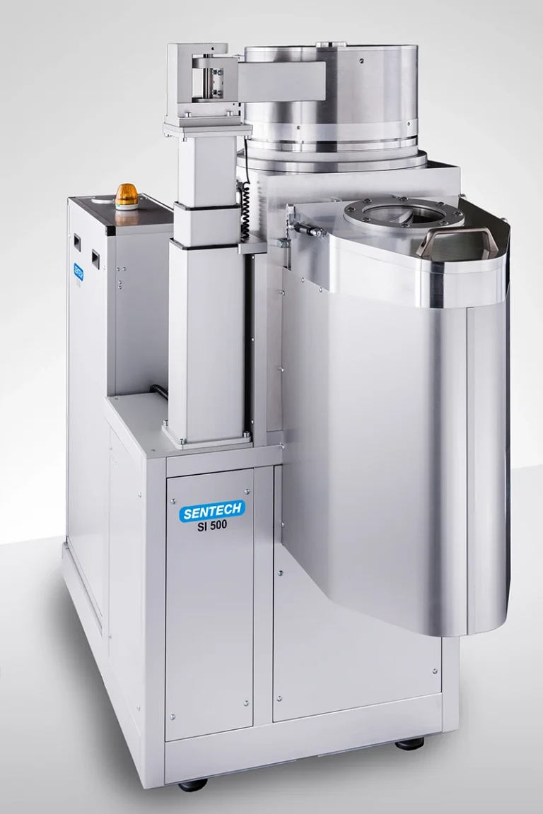
The SENTECH SI 500 ICP-RIE high-end plasma etch system uses an inductively coupled plasma (ICP) source with low ion energy for low-damage etch and nanostructuring.


Due to low ion energy and narrow ion energy distribution, low-damage etch and nanostructuring can be performed with the SENTECH SI 500 ICP-RIE Plasma Etch System.
High-rate plasma etching of Si for MEMS with a high aspect ratio is easily performed either using room temperature alternating processes or cryogenic processes for smooth side walls.
The SENTECH Planar Triple Spiral Antenna (PTSA) plasma source is a unique, high-end plasma process system feature of the SENTECH SI 500 ICP-RIE Plasma Etch System. The PTSA source generates uniform plasma with high ion density and low ion energy suited for low-damage etch of sensors, quantum dots, and HEMT. It features high coupling efficiency and very good ignition behaviour for processing a large variety of materials and structures.
Substrate temperature setting and stability during the plasma etching processes are demanding criteria for high-quality etching. The substrate electrode with dynamic temperature control in combination with He backside cooling and substrate backside temperature sensing provides excellent process conditions over a wide temperature range. Applications like recess and mesa etch in compound semiconductors demonstrate optimal process control, which is necessary for high device performance.

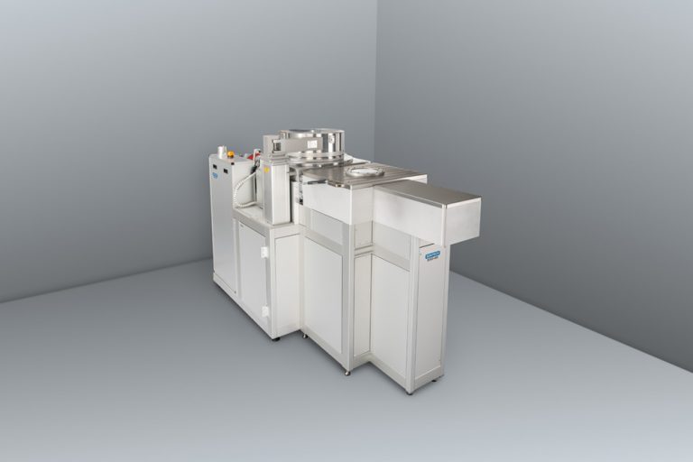
The SENTECH SI 500 ICP-RIE System represents the leading edge for ICP processing in both research and industry. The system comprises the ICP plasma source PTSA, a dynamic temperature-controlled substrate electrode, a fully controlled vacuum system, and a very easy-to-operate user interface. Configurations for processing a variety of materials, including but not limited to III-V and II-VI compound semiconductors (GaAs, InP, GaN, InSb), dielectrics, quartz, glass, silicon, silicon compounds (SiC, SiGe), and metals are achievable with this flexible and modular plasma etch system.
Low damage
20 nm SiGe nano wire
Nano structuring
AlGaAs / GaAs quantum dots
Cryogenic etching
Etching of silicon with SF6/O2 at -100°C
ICP power independent low energy distribution of PTSA plasma source
A large variety of substrates from 100 mm wafers up to 200 mm in diameter, as well as substrates on carriers, can be handled by the flexible load lock built into the SENTECH SI 500 ICP-RIE System. The single-wafer vacuum load lock guarantees stable process conditions and allows for straightforward switching of processes.
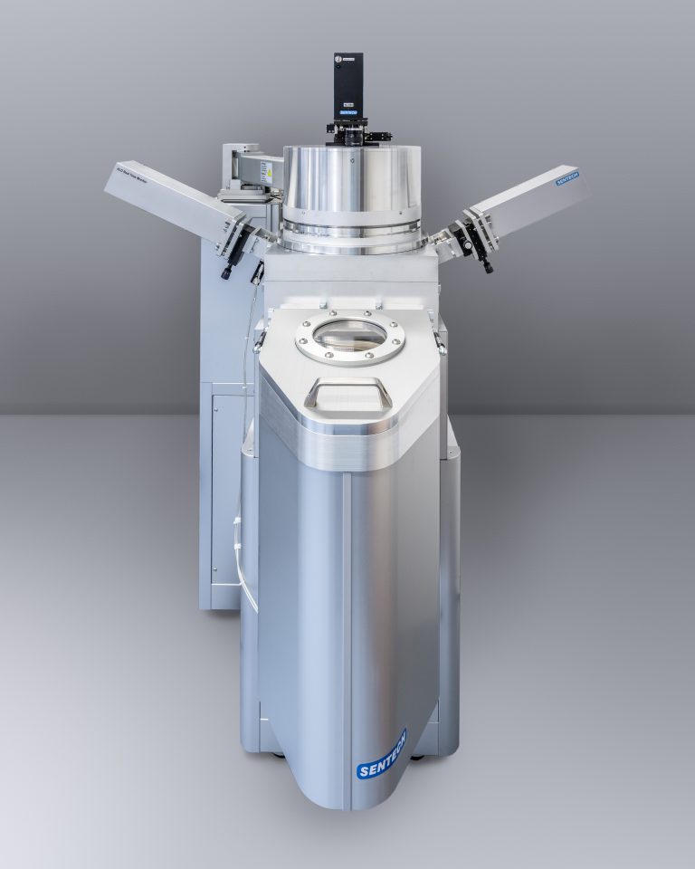
We can offer different levels of automation ranging from vacuum cassette loading to one process chamber up to a six-port cluster configuration, with different etch and deposition modules offering high flexibility and high throughput. The system can also be incorporated as a process module on a cluster configuration.
The SENTECH SI 500 ICP-RIE System is controlled by advanced hardware and SIA operating software, with a client-server architecture. A well-proven, reliable programmable logic controller (PLC) is used for the real-time control of all components.


Plasma etching enables the precise removal of materials from a substrate through chemical and physical reactions driven by ionised gases. Unlike traditional wet etching, which uses liquid chemicals and often produces isotropic profiles, plasma etching provides anisotropic, highly controlled material removal. For more information, click here.
SENTECH offer plasma etching systems to facilitate reactive ion etching (RIE), low-damage inductively coupled reactive ion etching (ICP-RIE), deep reactive ion etching (DRIE), cryogenic etching and low-damage atomic layer etching.
While many SENTECH systems are single-chamber tools, each dedicated to a specific process type (e.g., ICP-RIE for etch, ICPECVD for deposition), cluster-style configurations can bring multiple modules together under shared vacuum handling, letting you do different processes in sequence without breaking vacuum.
In general, you will need electrical power, compressed air, purging nitrogen, cooling water and a process gas supply and exhaust. You will receive an installation manual with your system, which will outline all of the specific requirements of your purchased system. Our technical service team are available to offer support and answer questions.
SENTECH has an international network of distributors and technical service experts. We deliver globally, including Europe, Asia, Africa, North and South America. For more details on in-country representation, click here
SENTECH has a large team of application experts for both plasma process technology and thin film metrology. At our campus are two laboratories which are used to process and characterise customer samples, for system demonstrations and customer training. SENTECH offers application support for the lifecycle of your system. Learn more about our application support or contact the team.
Yes, SENTECH has two application labs in-house. You can contact our application team, who will share with you all the details and provide a sample analysis form for you to complete. Click here for further information and contact details.
Yes, SENTECH has a large network of technical service experts who offer in-country support for both plasma process technology and thin film metrology systems. Remote or on-site support is possible depending on your requirements. Click here to find out more or to contact the team.
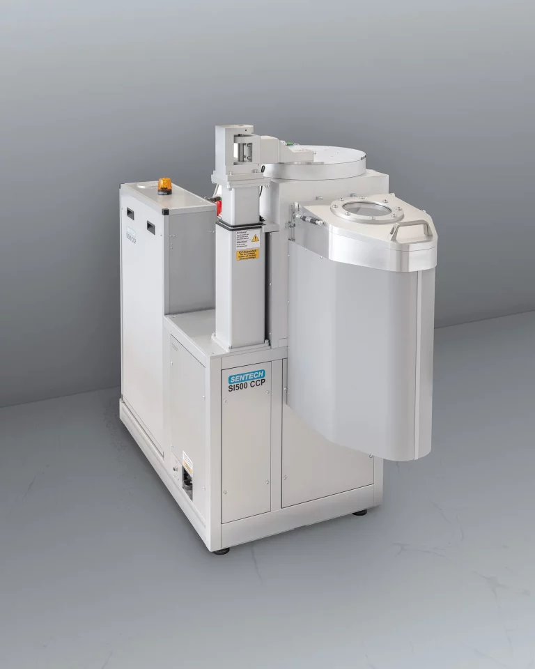
SENTECH provides process modules that combine multiple processes, such as SIPAR for PECVD and PEALD, in a single reactor. The SI 500 ICP-RIE accommodates chlorine and fluorine-based etch chemistry in one process chamber. These configurations come with dedicated hardware, cleaning and conditioning recipes, as well as training. These solutions prioritise a smaller footprint and cost efficiency while maintaining practical process repeatability performance.
Reactive Ion Etching (RIE) combines chemical etching with physical ion bombardment to deliver precise pattern transfer. In RIE systems, a plasma is generated between two electrodes using a radio frequency (RF) power source. Reactive species chemically react with the substrate surface while positive ions accelerate toward it, physically sputtering atoms away. Learn more about plasma etching processes.
Inductively Coupled Plasma Reactive Ion Etching (ICP-RIE) represents the next generation of plasma etching technology. It separates plasma generation and ion acceleration into two independently controlled systems:
This dual control enables deeper etching, improved anisotropy, and minimal substrate damage. Learn more about plasma etching processes.