The options of the SE 500adv support applications in many industries:
- Microelectronics
- Microsystems technology
- Photovoltaics
- Display technology
- Chemistry
Plasma Process Technology
Thin Film Metrology
The SE 500adv combines ellipsometry and reflectometry to eliminate the ambiguity of measuring layer thickness of transparent films.


The combination of ellipsometry and reflectometry allows for fast and unambiguous determination of the thickness of transparent films by automatic identification of the cyclic thickness period.
The combination of laser ellipsometer and reflectometry extends the thickness range for transparent films up to 25 µm or more depending on the photometer option chosen.
The multiple-angle manual goniometer with superior performance and angle accuracy enables the measurement of refractive index, extinction coefficient, and film thickness of single films and layer stacks.
The SENTECH SE 500adv combines ellipsometry and reflectometry to eliminate the ambiguity of measuring the layer thickness of transparent films. It extends the measurable thickness to 25 µm. Therefore, the SE 500adv extends the capability of the standard laser ellipsometer SE 400adv, especially for analysing thicker films of dielectrics, organic materials, photoresists, silicon, and polysilicon.
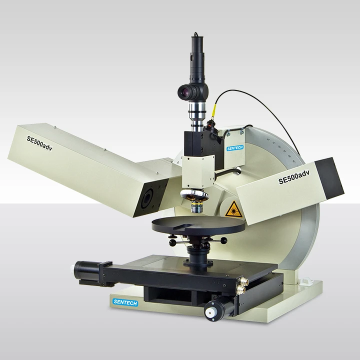
The SENTECH SE 500adv can be operated as a laser ellipsometer, as a film thickness probe, and as a CER ellipsometer. Consequently, it offers maximum flexibility never reached by standard laser ellipsometers. Operated as an ellipsometer, single and multiple-angle measurements can be performed. When operated as a film thickness probe, the thickness of a transparent or weakly absorbing film is measured under normal incidence.
The combination of ellipsometry and reflectometry (CER) in the SE 500adv comprises the ellipsometer optics, goniometer, combined reflection measurement head and auto-collimating telescope, sample platform, HeNe laser source, laser light detection unit, and photometer.
SENTECH has an international network of distributors and technical service experts. We deliver globally, including Europe, Asia, Africa, North and South America. For more details on in-country representation, click here.
SENTECH has a large team of application experts for both plasma process technology and thin film metrology. At our campus are two laboratories which are used to process and characterise customer samples, for system demonstrations and customer training. SENTECH offers application support for the lifecycle of your system. Learn more about our application support or contact the team.
Yes, SENTECH has two application labs in-house. You can contact our application team, who will share with you all the details and provide a sample analysis form for you to complete. Click here for further information and contact details.
Yes, SENTECH has a large network of technical service experts who offer in-country support for both plasma process technology and thin film metrology systems. Remote or on-site support is possible depending on your requirements. Click here to find out more or to contact the team.