Which plasma etching processes can SENTECH Systems carry out?
SENTECH offer plasma etching systems to facilitate reactive ion etching (RIE), low-damage inductively coupled reactive ion etching (ICP-RIE), deep reactive ion etching (DRIE), cryogenic etching and low-damage atomic layer etching.
What is plasma etching? Learn more about plasma etching processes
Plasma etching enables the precise removal of materials from a substrate through chemical and physical reactions driven by ionised gases. Unlike traditional wet etching, which uses liquid chemicals and often produces isotropic profiles, plasma etching provides anisotropic, highly controlled material removal. For more information, click here.
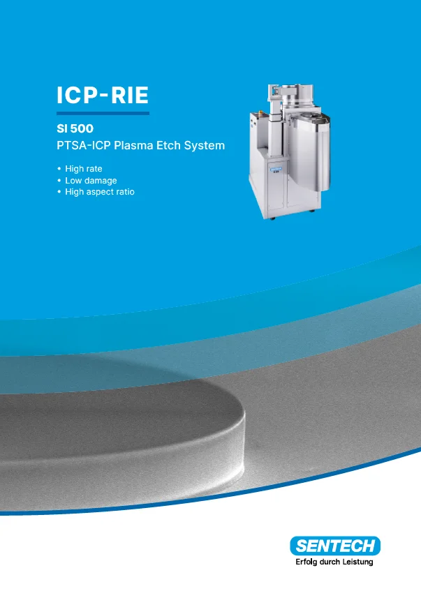
SENTECH SI 500 ICP-RIE Brochure
SI 500 ALE
ICP-RIE with atomic layer etch system Precise ion energy control with low ion energy of PTSA combined with high-precision bias control Efficient gas control and switching Process monitoring with SENTECH Real Time Monitor optional
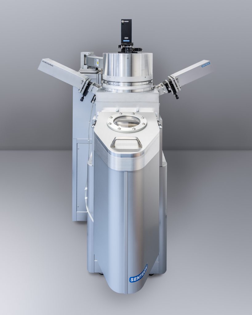
SI 500 CCP
RIE plasma etch system Smart solution for He backside-cooled etching Capacitively coupled plasma source, upgradable to ICP plasma source PTSA 200
SI 500 DRIE

Deep reactive ion etch system for gas chopping process Fast gas replacement for low scalloping and smoother sidewalls Efficient ICP source coupling for fast etch rate For up to 150 mm wafers
SI 500 400
ICP plasma etch system for multi-wafers and large substrates With vacuum load lock For up to 380 mm wafers
SI 500 C

Cryogenic ICP plasma etch system With vacuum load lock Substrate temperature from -150 °C to 80 °C (LN2 cooling) Substrate temperature -10 °C to 150 °C for Bosch process with circulation chiller (optional) Automatic switching unit for comfortable change between cryogenic etch and Bosch process
SI 500

ICP-RIE plasma etch system With compact vacuum load lock For up to 200 mm wafers Substrate temperature from -20 °C to 250 °C Optional: -30 °C to 200 °C
SI 500 ICP-RIE System
The SENTECH SI 500 ICP-RIE high-end plasma etch system uses an inductively coupled plasma (ICP) source with low ion energy for low-damage etch and nanostructuring.