Ellipsometry is a cornerstone of thin-film metrology, semiconductor and nanotechnology quality control. Techniques such as spectroscopic ellipsometry, laser ellipsometry, and reflectometry each offer distinct advantages, enabling accurate optical and structural analysis at the nanoscale. As device architectures continue to shrink and material stacks grow more complex, ellipsometry is set to remain an essential tool for ensuring precision, consistency, and performance in advanced manufacturing.
Principles, Origins, and Modern Applications
Ellipsometry is a high-precision optical metrology technique used to characterise thin films by determining their thickness, refractive index, and optical constants. It operates by measuring changes in the polarisation state of light upon reflection from, or transmission through, a material surface.
The foundations of ellipsometry date back to the late 19th century, when Paul Drude and other pioneers of optical physics first described the interaction of polarised light with matter. However, ellipsometry emerged as a practical analytical technique in the mid-20th century with advances in polarisation optics and computational modelling. Its adoption accelerated rapidly alongside the rise of semiconductor manufacturing, where nanometre-scale control of thin films became essential.
Today, ellipsometry is valued for its non-destructive nature, extreme sensitivity, and applicability to films only a few angstroms thick. These attributes make it indispensable in semiconductor fabrication, optical coating analysis, photovoltaics, and advanced materials research.
Modern devices, from integrated circuits to solar cells, depend on precisely engineered thin-film stacks. Even sub-nanometre deviations in layer thickness or optical properties can significantly impact performance, positioning ellipsometry as a critical tool for both process optimisation and quality assurance.
Fundamental Principles of Ellipsometry Measurement
At its core, ellipsometry quantifies how the polarisation state of light changes when interacting with a film-covered substrate. The technique measures two key parameters: Ψ (Psi), representing the amplitude ratio, and Δ (Delta), describing the phase difference between the p- and s-polarised light components, where p- and s- refer to light polarised parallel and perpendicular to the plane of incidence, respectively.
Ellipsometric measurement is based on these changes in the polarisation state of light upon reflection, rather than absolute reflected intensity. These changes are expressed as ratios of reflected field components. The measurement is inherently self-referenced. As a result, ellipsometry does not require an external reference measurement or intensity calibration, as used in reflectometry techniques.
By fitting these measured parameters to optical models, researchers can extract film thickness, refractive index, extinction coefficient, and layer uniformity. This non-invasive yet highly sensitive approach provides detailed insight into the optical and structural properties of complex transparent and semi-transparent material systems.
How to Choose the Right Ellipsometry Technique
Selecting the optimal ellipsometry method depends on material and film complexity, parameters, and measurement speed. In semiconductor manufacturing and materials research, ellipsometry is implemented through measurement approaches designed to address both detailed material characterisation and stringent process-control requirements. Spectroscopic ellipsometry is widely used in research and process development, as its broadband, wavelength-resolved measurements enable precise extraction of optical constants, film thickness, and multilayer stack properties across complex material systems. Laser ellipsometry, by contrast, employs monochromatic, highly coherent light to deliver exceptional measurement stability and speed, making it particularly well suited for in-line and in-situ monitoring during deposition and etching processes. The following sections discuss these techniques in greater detail, outlining their underlying principles, performance characteristics, and roles in advanced semiconductor and materials applications.
Spectroscopic Ellipsometry, Broadband Optical Metrology for Thin-Film Characterisation
Spectroscopic ellipsometry analyses polarisation changes across a broad wavelength range, typically spanning the ultraviolet (UV), visible (VIS), and near infrared (NIR) regions. This wavelength-dependent information enables the comprehensive determination of optical constants and thickness, even for complex multilayer structures.
A broadband light source illuminates the sample, and the reflected or transmitted light is analysed spectrally. By fitting the measured Ψ and Δ spectra to physical dispersion models, researchers can derive additional parameters such as bandgap energy, composition gradients, and surface roughness.
Spectroscopic ellipsometry is especially valuable in semiconductor and thin film process development and control. Common applications include gate oxide thickness monitoring, photoresist characterisation, and multilayer dielectric or metal stack analysis.
Its combination of high accuracy, non-contact operation, and sub-nanometre sensitivity makes spectroscopic ellipsometry ideal for both research environments and industrial settings where detailed material insight is required.
Laser Ellipsometry, High-Precision, Monochromatic Film Measurement
Laser ellipsometry is a specialised form of ellipsometry that uses a monochromatic, coherent laser source rather than broadband illumination. The laser’s high stability and coherence significantly enhance the signal-to-noise ratio, enabling extremely precise detection of thin films and subtle surface changes.
Unlike spectroscopic ellipsometry, which captures full spectral information, laser ellipsometry typically operates at a single wavelength or a small set of discrete wavelengths. Systems such as the SENTECH AL Real Time Monitor are particularly well-suited for real-time, in-situ process monitoring during deposition, etching, or thermal treatment steps. By analysing polarisation changes of the reflected laser beam, laser ellipsometry provides rapid feedback on film growth rates, thickness evolution, and surface reactions.
Ellipsometry in Semiconductor Manufacturing and Process Control
Ellipsometry plays a central role in modern semiconductor fabrication, where tight dimensional tolerances and material consistency are essential. Throughout wafer processing, numerous thin films are deposited, etched, or thermally grown, each requiring precise characterisation.
Key applications include gate oxide thickness control in CMOS devices, monitoring layers, and photoresist analysis during lithography. Ellipsometry also enables wafer-scale uniformity assessment, helping manufacturers maintain consistent film properties across production lots.
By detecting process drift early and providing actionable feedback, ellipsometry supports real-time quality control. Its non-destructive nature makes it suitable for both R&D and high-volume manufacturing, where continuous in-line monitoring improves yield and reduces cost.
Enabling Advanced Technologies with Ellipsometry
Ellipsometry provides precise, non-destructive measurements of thin film thickness and optical properties, making it a versatile technology for use in a broad range of industries. In the semiconductor industry, it plays a key role in the characterisation of dielectric materials such as SiO₂ and SiNₓ, as well as advanced structures including silicon-on-insulator (SOI), MEMS devices, and emerging materials such as graphene and other two-dimensional materials (e.g. transition metal dichalcogenides (TMGs).
In display technology, ellipsometry is commonly applied to multilayer stacks involving glass or polyimide substrates, transparent conductive oxides such as ITO, colour filter layers, and organic light-emitting diode (OLED) structures. In photovoltaics, it is used to monitor and optimise advanced solar cell architectures, including PERC, TOPCon, and heterojunction (HJT) technologies.
The automotive sector employs ellipsometry in the development and quality control of MEMS components, power electronic devices for electrical conversion technology, and optical coatings used in car headlights. In the glass industry, applications include the characterisation of low-emissivity (low-E) coatings on flat glass, photovoltaic glass, and functional diffusion barriers or transparent conductive oxide (TCO) layers.
In the lighting industry, ellipsometry is used for the analysis of LED and OLED structures, including transparent electrode layers such as ITO. Optical applications include the design and control of dielectric anti-reflective coatings and bio-inspired surface structures such as moth-eye textures.
In the life sciences, ellipsometry is applied to the study of thin organic and biological layers, including protein adsorption, biomolecular interactions, and functionalised surfaces for biosensors. Its sensitivity to sub-nanometre thickness changes makes it a valuable tool for investigating surface chemistry, bio interfaces, and film formation processes in both research and applied biomedical contexts.
Reflectometry vs Ellipsometry
Reflectometry is another widely used optical technique for thin-film measurement. Instead of analysing polarisation, reflectometry measures reflected light intensity as a function of wavelength or angle. While it offers faster measurements and simpler analysis, it provides less information about refractive index, anisotropy, and multilayer complexity. As a result, reflectometry is often deployed alongside ellipsometry. In high-throughput QC environments, such as wafer inspection or resist thickness verification, it provides rapid thickness feedback, while ellipsometry delivers deeper optical insight for complex materials.
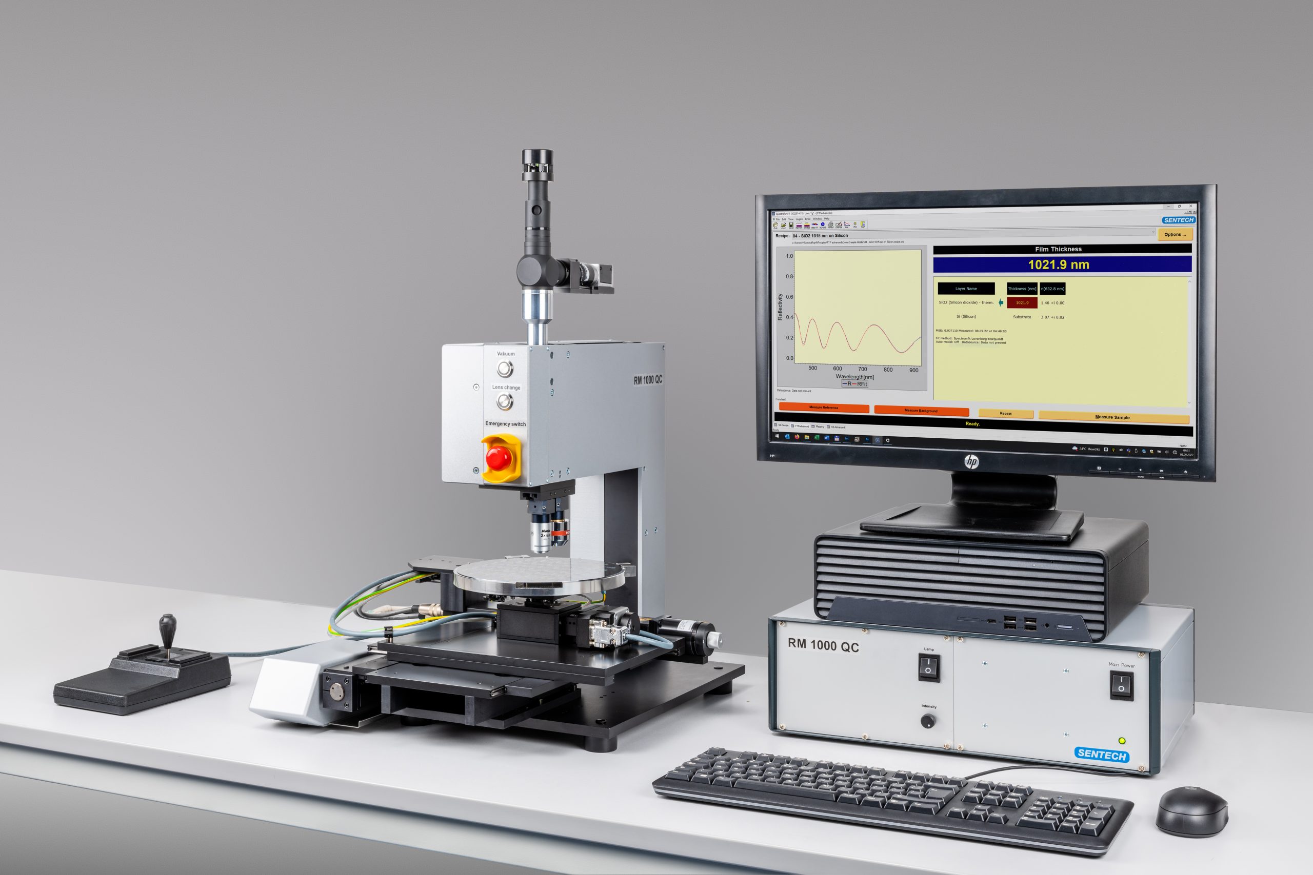
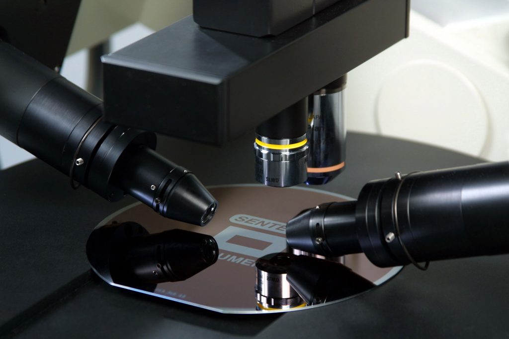
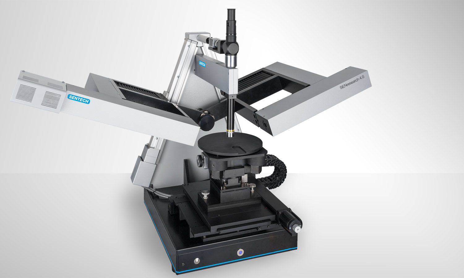
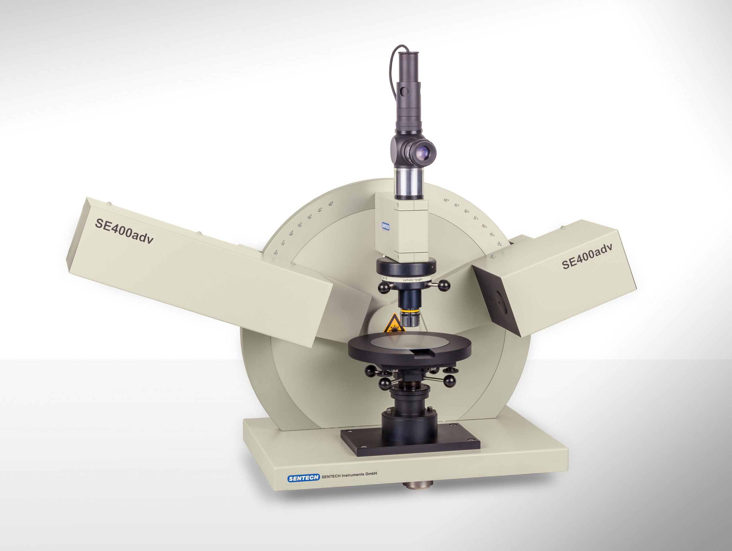
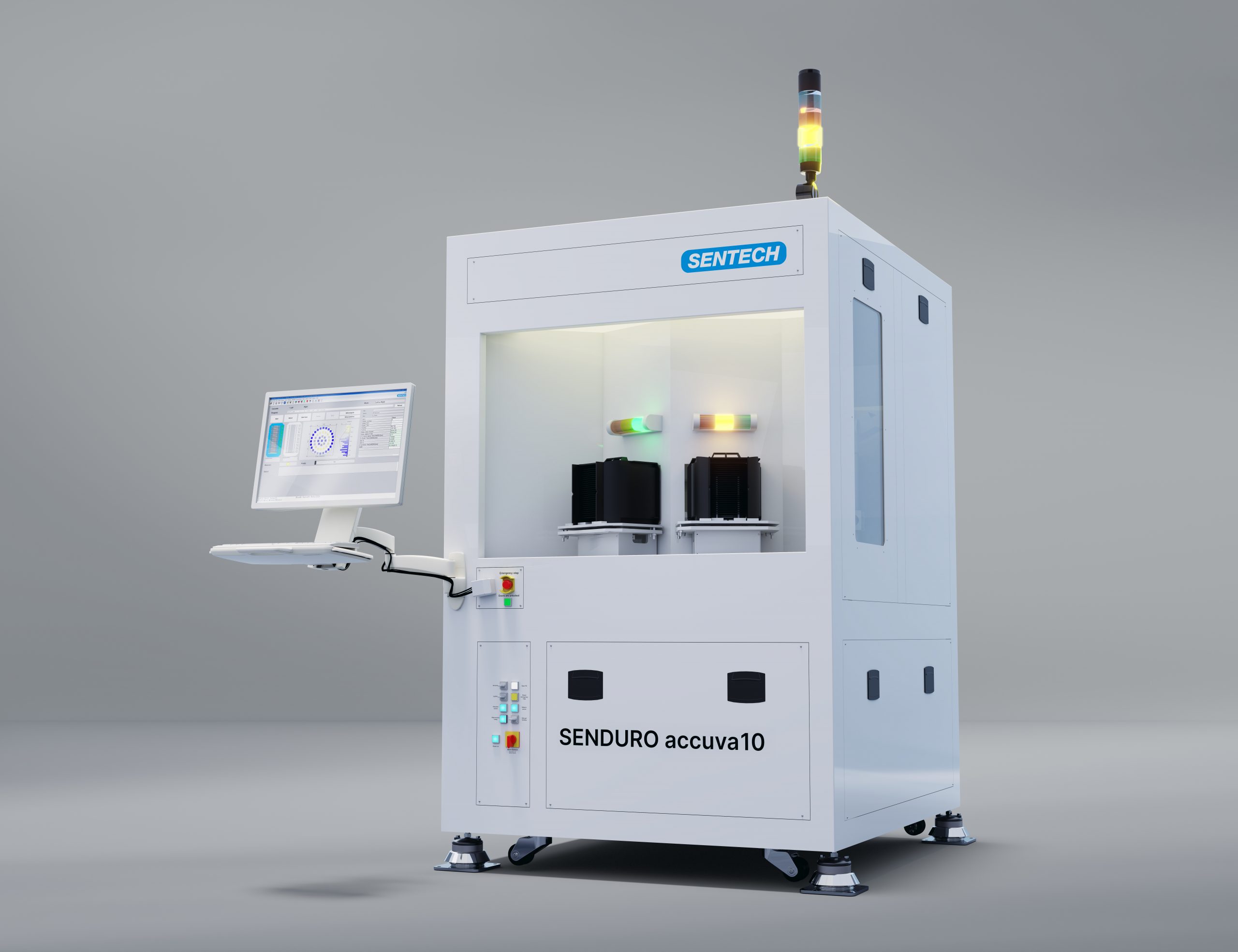
SENTECH Ellipsometry Solutions for Research and Production
The SENTECH ellipsometry product portfolio includes high-performance spectroscopic ellipsometry, laser ellipsometry, reflectometry and in-situ systems for thin-film measurement and quality control. These tools combine robust hardware with advanced modelling software for both research and industrial use.
SENTECH systems are developed specifically to meet the demands of scientific accuracy, production-ready reliability, and scalable metrology solutions in thin-film coatings, optical layers, and nanotechnology applications for the semiconductor industry. Modular designs support in-line, mapping, and in-situ monitoring configurations, delivering sub-nanometre precision, broad spectral coverage, and flexible measurement workflows.