Skip to content
Products
Close Products
Open Products
Application and Industries
Close Application and Industries
Open Application and Industries
Company
Close Company
Open Company
Careers
Customer support
Close Customer support
Open Customer support
Plasma Process Technology
Plasma Etching
PECVD Systems
Atomic Layer Deposition
Cluster Configuration
Menu
Plasma Etching
PECVD Systems
Atomic Layer Deposition
Cluster Configuration
Thin Film Metrology
Spectroscopic Reflectometry
Laser Ellipsometer
Spectroscopic Ellipsometry
Metrology for Quality Control
In-situ Metrology
Menu
Spectroscopic Reflectometry
Laser Ellipsometer
Spectroscopic Ellipsometry
Metrology for Quality Control
In-situ Metrology
Optoelectronics
MEMS
Sensors
Power Devices
Quality Control
Menu
Optoelectronics
MEMS
Sensors
Power Devices
Quality Control
News
Events
Menu
News
Events
Worldwide Sales Network
Application Support
Technical Service Support
Menu
Worldwide Sales Network
Application Support
Technical Service Support
Search
Search
Close this search box.
Contact
Home
>
Products
>
Plasma Process Technology
Plasma Etching
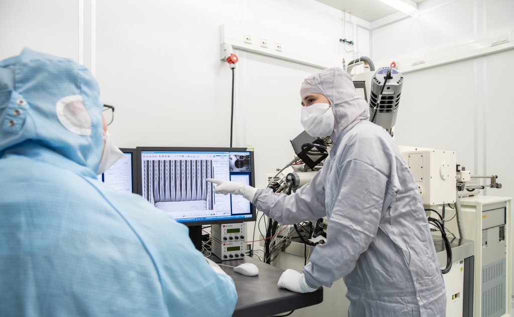
Discover the SENTECH modular and flexible ICP-RIE processing systems for low-damage, high-rate, and high-selectivity inductively coupled plasma (ICP) etching.
Plasma etch systems
ICP-RIE Plasma Etch System –
SI 500
The SENTECH
SI 500
ICP-RIE high-end plasma etch system uses an inductively coupled plasma (ICP) source with low ion energy for low-damage etch and nanostructuring.
Cryogenic ICP-RIE Plasma Etch System –
SI 500
C
The
SI 500
C
represents the leading edge for inductively coupled plasma (ICP) processing designed for cryogenic etching.
RIE Open Lid Plasma Etch System –
Etchlab 200
The plasma etching system
Etchlab 200
features the benefits of cost-effective direct loading for RIE.
RIE Plasma Etch System with Small Footprint –
SI 591 compact
The SENTECH
SI 591 compact
RIE Plasma Etch system with load lock is a compact solution for chlorine and fluorine-based RIE.
RIE Plasma Etch System with He Backside Cooling –
SI 500
C
CP
A conductively coupled plasma etch tool with Helium backside cooling for processing of substrates in RIE mode.
Plasma Process Technology
PECVD
Systems
Atomic Layer Deposition
Cluster
Configuration
News
Wafer-level integration challenges of ALD for 2D materials
Find out about the collaboration between SENTECH and the Ruhr-Universität Bochum (RUB).
Analysing the earth’s heat balance to better understand global warming
The European Space Agency's satellite mission planned for 2027.
The SENTECH “Plasma Process Technology Seminar” 2024
Click here to find out more about the SENTECH Plasma Process Technology Seminar.
The SENTECH Thin Film Metrology Seminar and Workshop
Read the full article to find out more about the seminar.
SENTECH set to expand sales and service offerings in Spain
Welcome to the SENTECH team Izasa Scientific
Products
Plasma Process Technology
Thin Film Metrology
Plasma Process Technology
Thin Film Metrology
Application and Industries
Optoelectronics
MEMS
Sensors
Power Devices
Quality Control
Optoelectronics
MEMS
Sensors
Power Devices
Quality Control
About SENTECH
Careers
Customer Support
Contact
About SENTECH
Careers
Customer Support
Contact