


Silicon Carbide (SiC) is a widely used semiconductor material for power device applications. A SiO2 mask is generally used for the etching of SiC structures up to a few micrometres deep. The selectivity of the SiO2 mask usually becomes a limiting factor for deeper SiC etching. Thus, hard metal masks like Ni are normally introduced for deeper SiC etching. These materials intrinsically provide a much higher etch selectivity but have a major drawback which is the non-volatility of their etch by-products. Mask redeposits on the SiC surface and its sidewalls can lead to unwanted micro-masking.
A SiC plasma etch process using a SiO2 mask does not face this problem. Thus, a higher etch selectivity to the SiO2 mask can be of high interest when it comes to deep SiC etching while keeping a reasonable SiO2 mask thickness.
Using the SENTECH SI 500 ICP-RIE System, a high etch rate and increased selectivity to the SiO2 mask are achieved due to the proprietary SENTECH Planar Triple Spiral Antenna (PTSA), a unique inductively coupled plasma (ICP) source that provided high plasma density. A vertical sidewall profile is maintained, simultaneously.

AlGaN/GaN heterostructure-based high electron mobility transistors (HEMTs) are currently under development for high-power and high-frequency applications. These transistors utilise a two-dimensional electron gas (2DEG) channel, offering high carrier density and mobility. The main process challenge lies in minimising energy loss without compromising the device’s performance, necessitating a precise nanoscale thickness etching process.
Atomic layer etching (ALE) is a repetitive process consisting of two consecutive, surface reaction steps. The first surface reaction step involves modifying the surface, followed by removing the modified layer at lower ion energies. This process achieves the atomic-scale etching necessary for the AlGaN layer. However, developing the ALE process with sub-nanometer precision is still a relatively new and challenging technique. Therefore, it’s crucial to have real-time, in-situ monitoring capabilities to set up the process and promptly understand relevant surface reactions and the pssibility to conrol ion energies and distribution.
The SENTECH SI 500 with the ALE option includes the proprietary Planar Triple Spiral Antenna (PTSA), a unique inductively coupled plasma (ICP) source. The PTSA enables control of the ion energy distribution and ion energies during the etching process. Having this control is advantageous for both the modification and removal steps essential for successful ALE. Additionally, the SENTECH AL Real Time Monitor in-situ laser ellipsometer provides detailed process development and fully software-integrated real-time process observation.
The successful ALE of the AlGaN layer in AlGaN/GaN heterostructures was achieved using the SENTECH SI 500 with the ALE option. The AlGaN structure underwent cyclic surface modification followed by the removal of the modified layer. To demonstrate the ALE characteristics, a synergy test was conducted. Finally, post-etch surface roughness was investigated using atomic force microscopy (AFM), and a flat and smooth surface was achieved for this ALE process at room temperature.
Dielectric materials such as SiNX, SiO₂, HfO₂, Al₂O₃ and photoresists on SiC wafers harness the electrical, thermal, mechanical and chemical advantages of both materials, resulting in a highly versatile platform that can address the needs of a wide range of advanced technological applications. This synergy between these dielectric materials on SiC makes them particularly valuable in scenarios where extreme conditions and high performance are essential. These make dielectrics on SiC wafers extremely suitable for high-power, high-frequency, and high-temperature applications in various semiconductor devices, such as power electronics, telecommunications, and automotive electronics, as well as other emerging fields.
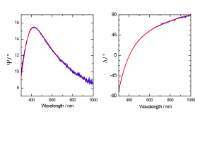
Ellipsometry is a precise and versatile tool for characterising
dielectric layers such as SiO₂, HfO₂, Al₂O₃ and photoresists on SiC substrates. Ellipsometry provides an accurate and reliable quality control measure during the fabrication of SiC-based semiconductor devices, ensuring that the material meets the desired specifications and standards for applications in semiconductor devices used in power electronics. The challenges of backside reflection (BSR) can be met using the flexible, versatile and accurate SENTECH SENDURO accuva10. The tool successfully demonstrated a precise measurement of dielectric materials on SiC wafers with no interference fringing and no position-dependent variation of the dispersion of n, k of SiC.